
PCB | manufacturing process | 2-layer
PCB production
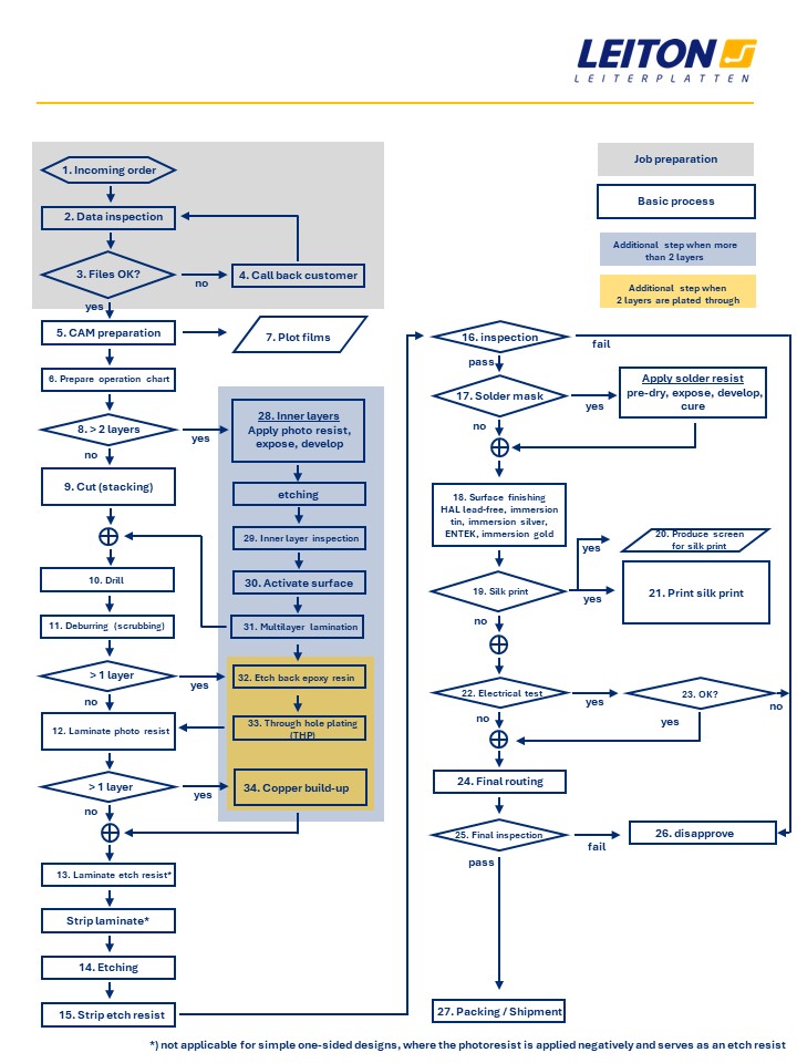
The Printed Circuit Board (PCB) production requires many different steps in fields of mechanical, photo sensitive, galvanic and chemical processes. The complete process of printed circuit board production (PCB production) for a double layer PCB is as follows:
To take an order for the PCB production, the PCB manufacturer needs the following data and information:
- Gerber files or other layout files to convert into PCB production files, e.g. Eagle, Target3001, KiCAD, Orcad, Sprint, Protel etc.
- Quantity
- Lead time
- PCB thickness (0,1 mm to about 4,2 mm. Standard is 1,6 mm)
- PCB base material (FR4, TG-value, CEM, Alu-IMS, Rogers, Isola, or other special PCB base material types)
- Final copper thickness (35µm to 400µm copper thickness)
- Number of layers, if not clearly defined by Gerber files
- Single PCB or panel type/size
- Mechanical processes (V-cut, routing, punching, bevelling etc.)
- Surface finish: HAL, immersion tin (Sn), immersion gold (NiAu)/ENIG, immersion nickel-palladium-gold (ENEPIG), immersion silver (Ag), finger gold/hard gold, OSP etc.
- Solder mask (desired colour, standard colour is green)
- Silk print, if needed (desired colour, standard colour is white)
- Electrical test (E-test) or other tests, e.g. resistance measurements, impedance control etc.
The check of the PCB layout files is commonly known as the design rules check (DRC). First, the PCB layout is checked for completeness. Second, the relevant characteristics for the PCB production are checked and may be corrected. For example, the following are checked during DRC:
- Pads cantered to drills "snap pads".
- Check annular rings of copper around the drills.
- Smallest drill size according to technology.
- Check trace width/gaps according to capabilities or ordered technology range. Standard is 6mil-Technology (ca. 0,15mm). Sometimes 4mil and smaller is required.
- Swell traces for etching, to avoid diminution during PCB production.
- Separation of plated (PTH) and non-plated drills (NPTH) into different drill programs.
- Clear routing or V-cut outlines from copper areas to avoid burr.
- General plausibility check (any trace intersections, missing drills etc.)
- Swell solder mask (mostly bigger than copper pads) and close too small distances.
- Check outline for breaks, insert panel breakaways and set different routing tools.
- Optimize drill and routing path to save time during PCB production.
According to the capability or the ordered technology, the layout files are checked for plausibility and feasibility. Limits araise due to differences in PCB production processes and required materials for different PCBs. If these limits are exceeded and it is not possible to correct them according to the design rules, the customer will be notified. Design rules checks never include the functional test of the electronic device itself. It only focuses on the PCB production. Thus the PCB layout files are considered being acceptable, when all design rules are met.
In case of uncertainties about the PCB production files, the customer will be informed to clarify the matter. The customer is contacted by email or phone depending on the urgency. The advantage of emails is that we can attach screenshots and visualize the problem.
When the preparation of the single PCB layouts for production is finished, several things have to be added into the different layers and files. This additional information is needed for the machines in production and differs from each PCB supplier. Different fiducials and copper areas will be added into the film files as well as IDs and names. Registry holes will be added into the drill and routing files before converting into Sieb & Meyer or Excellon. The most common CAM software for PCB production is:
- CAM350 (https://www.cadcompact.de/index2.htm)
- Genesys 2000
- UCAM
- CAMMaster, ehemals Lavenir (https://www.pentalogix.com
The operation chart contains all important information for PCBs production: PCB specifications, work procedures, quantities, and lead times. The more sophisticated procedures and special materials are used, the more important is a highly accurate operation chart for the PCB production. The operation chart is the most important part in PCB production and the responsible person needs a lot of experience to prepare it. In this step, the course for a reliable and precise PCB production to meet the customer expectations is set.
Industrial PCB production require films. These films are mostly plotted in a laser plotter and contain the structures of the different layers (copper, solder mask, silk print etc.). Sometimes control films are produced to show the drills and the exact outline of the PCB. The films are developed in a darkroom after plotting. Silver films and diazo films are in use. Some high-tech applications with very high demands in accuracy plot the structures on glass. The advantage of glass is that the material is very consistent in its size. Diazo films are used for normal serial production. Silver films are used for prototype PCB production only, because the abrasion is higher.
Supplier for PCB film plotters:
Mania Technologie AG - www.mania.de
PCBs with more than two layers are commonly called "multilayer PCBs". Multilayer PCBs have to run through several production steps before being treated like common two-layered PCBs.
PCB base materials are mostly produced and delivered to the PCB supplier in large boards (too big for production). The supplier has to cut them into the production size with a punch cutter. Damageable PCB base materials e.g. ceramic materials for high frequency applications have to be cut with a routing machine. The size of the panel depends on the production processes and the machine capacities of the PCB manufacturer. Serial production suppliers usually produce bigger panels (around 500 x 600 mm) whereas prototype PCB productions use panel sizes around 300 x 400 mm. Some PCB manufacturers have fixed panel sizes (mostly serial production) which exactly match each machine configuration in the production. To save time, the base material panels are sometimes put into packages prior to drilling. E.g. 2 to 4 panels of 1,6mm base material with a thin 0,15mm aluminum cover on top and a 2mm pressboard on the bottom make one package. This allows drilling several PCBs in one process.
The packaging is mainly limited by the drill diameters. Small drill sizes limit the package thickness. This is one reason, why small drill sizes are more expensive in mass production (e.g. smallest drill <0,6m drill = 2-panel package / >=0,6mm = 3-panel package). The aluminum cover on top is responsible to "grease" the drill tool for a straighter hole. The pressboard on the bottom keeps the distance to the machine table so to prevent the tools from drilling into it.
The PCB panels are drill in packages. To fix the package on the machines, different kind of styluses are in use. Loading of the machine can happen manually or automatically with a loader at the back side, simultaneously holding many panels. The machine drills the hole according to the drill program and changes the tools automatically. The speed of drilling depends on the tool size. Small drills turn faster, but the hits into the PCB package are slower.
Information and supplier for PCB drill machines:
Schmoll Maschinen GmbH - www.schmoll-maschinen.de
Multilayer PCB drilling
Before the drilling process of multilayer PCBs, the inner layer is inserted by pressing the packages. Thus the drills must percisly hit the center of its designated position. Otherwise pads in the inner layers are not connected well, or more likely: the drill offset contacts two different potentials (VCC & GND) which will lead to a short after the plating process. The difficulty in the drilling process is accuracy without visual targets. The outer layers have a complete copper area, so the structures can only be seen by modern x-ray drill machines. PCB suppliers with non-x-ray drill machines have different ways to counter this problem. Some drill one sample blindly and etch it copper free afterwards, enabling them to see the offset and correct it for the following boards. This is a more expansive but more accurate way then the other way in use: scrubbing the sides of the PCB panel to make only the targets visible in the inner layers. The board remains intact, but nonlinear offsets cannot be corrected here. More ways to counter this problem are in practical use. Almost every PCB supplier has its own process for this as well as its own philosophy what is best and why.
Drilling blind vias
Some special multilayer PCB applications require plated drills, which do not run through the whole PCB. With blind vias you can connect outer layers with only one, some, or all inner layers without connecting the other outer layer. Because you can not see through these holes, they are called "blind vias". This process is a bit more complicated, takes more timeand thus is more expensive. First, you can not drill the panels in packages, because the drill tool has to stop at a certain x-axis value for each single PCB. Second, it is more difficult to get liquids inside blind vias, because air bubbles cannot be easily removed out of these holes. This phenomenon depends on the aspect-ratio. Commonly an aspect-ratio of 1:1 is no problem in PCB production. This means, that the drill size can equal the depth of the blind via. Extreme aspect-ratios with thin and long holes are more difficult to produce.
Drilling buried vias
Drilling of blind vias is a sequence of additional processes in the multilayer PCB production but nothing which requires more sophisticated equipment. Before pressing the multilayer the buried vias have to separately drill into the inner layers (packing is possible). After drilling the blind vias, the inner layers are plated and plugged. If more than just two inner layers have to be connected with buried vias, an additional pressing process is required. After pressing the outer layers on the inner layers with the buried vias, these buried vias are not visible from the outside anymore, they are "buried". Although this process is not a complicated one, the costs are much higher than for standard multilayer PCBs. The costs mainly refer to the higher complexity of the process, the organization and the required time.
After the drilling process the PCBs have to scrubbed to remove burr. Besides removing burr by scrubbing, the copper surface is cleaned and abraded. The abraded copper surface supports the adhesion of the photo resist laminate.
Information and supplier for drill cleaning processes of: Höllmüller Maschinenbau GmbH - https://www.hms-germany.de/
To superimpose the PCB structures on the printed circuit board either an UV sensitive laminate is pressed on the boards with heat, or a thin liquid lacquer is casted over the PCB and dried in an UV oven. Now the plotted films are used. Some machines automatically adjust the film to some target holes on the PCB. Other suppliers still use the manual adjustment. A new method is direct exposure of the laminate. Therefore no films are used, but the exposure machine uses a laser and draws the PCB structures on the laminate individually. The exposed areas harden and the unexposed areas are uncovered after developing the laminate.
The exposed copper areas are covered with with galvanic tin or other etch resistant materials. These surfaces prevent the covered areas from beeing etched away. Afterwards the photo resist is removed from the other areas which exposes the blank copper underneath
The copper is etched with an acid or alcalic liquid. In the industrial PCB production mainly ammonium chloride containing copper chloride dilution is used. Etching of copper increases the copper concentration in the dilution. To keep the copper ions at a constant pH-value of about 8,5, ammonia is used to keep the copper tetramin complex.
Information and suppliers of PCB etching systems:
- Atotech Germany GmbH - www.atotech.com
- Enthone GmbH - https://www.enthone.com/de
- Höllmüller Maschinenbau GmbH - https://www.hms-germany.de/
Tin is mainly removed with hydrochlorid acid or nitric acid. After this etching process the PCB is fully electrically functional.
Information and supplier of PCB etching systems:
- Höllmüller Maschinenbau GmbH - https://www.hms-germany.de/
The optical inspection can be done manually with a lighted magnifier or automatically optical inspection is used (AOI). The AOI is filming the PCB structures and compares it to the layout files. The computer shows the discrepancies of the PCBs and the user can fix them (e.g. scratching away a short) or reject the inner layer.
Information and supplier of AOI systems for the inspection of PCBs:
- Orbotech Ltd. - www.orbotech.com
Solder mask is used to allocate tin only on the soldering spots. This prevents eventual shorts of the tin after soldering processes. The complete name "solder stop mask" explains more accurate, what this layer is actually doing. Solder materials like tin do not cling to the PCBs on areas with solder stop mask. By the way this solder mask gives PCBs the typical green colour. Nowadays almost every other colour is possible but is often a bit expensive. The solder stop mask is superimposed with a thin lacquer casting machine or by silk printing. The lacquer is pre-dried first and then exposed with the solder mask films like the copper structures have been exposed (exposure time differs). The PCBs are developed and the solder mask is dried again. Because of the drying processes this procedure may take a long time (up to 2 hours, depending on the ovens) and is critical for PCB express services. For some cases a solder laminate is used instead of the liquid lacquer. The advantage is, that holes of up to 3mm diameter can be covered with it. This is important for some vacuum adapter PCB assembly machines.
Information and suppliers of solder mask for PCBs:
Peters GmbH & Co. KG - www.peters.de
The surface finish of PCBs in the production mainly differ in the process of precipitation.
HAL
For the HAL process (Hot Air Leveling) first the complete PCB is covered with flux. Then the PCB is plunged into a hot tin bath, which covers all copper areas. The PCB remains inside the bath for several seconds with a temperature of around 260°C. When the PCB is lifted out of the bath, hot air blows the still liquid tin out of the holes with high pressure. This gives the process its name. The advantages of this process are the speed of the procedure and the relatively thick tin surface making it perfect for multiple soldering in OCB assembly. Disadvantages are the extreme thermal strain of the material and the problem of uneven tin surface for fine pitch components.
Immersion tin
Immersion tin is precipitated in a bath or in a horizontal covering machine. The process takes more time than HAL but generates a planar surface, perfect for fine-pitch assembly. The disadvantage of immersion tin is the limited capability of multiple soldering processes, due to its thinner tin surface. It is also not very suitable for storage and should be assembled and solder as soon as possible after the PCB production.
Immersion silver
Similar to immersion tin, this process precipitates silver on the PCB inside a bath or by horizontally moving through a machine. Immersion silver has the reputation to be even more sensitive than immersion tin. Dirt or finger prints can easily effect the solder ability.
OSP
OSP (Organic Solderablity Preservative) is used to cover copper areas and prevent oxidation. To solder components on the OSP-covered copper pads, tin has to be added later. This surface finish is mainly used in cheap mass production products for toys and consumer electronics, where every gram of tin is critical to the price. Unfortunately this surface finish faces prejudice due to low quality OSPs in the early beginnings. Nowadays it is hardly in use in western Europe thus not in the product range of most PCB suppliers.
Immersion gold
Immersion gold is the best surface finish in almost all reagards. Fine-pitch components are easily assembled, multiple solder processes can be made, long term storage is possible, and bonding is possible. The disadvantage is mainly the costs for this most expensive surface finish. These costs do not primarily arise because of the gold price itself. Actually the costs for the much thicker nickel coating below the gold can be even higher (ctandard NiAu consists of 0,3 to 0,5µm gold over 4µm nickel). The costs emerge from the very sensitive process of immersion gold and its difficulty to keep it within operating values.
Information and supplier PCB surface finishing:
Atotech Germany GmbH - www.atotech.com
Enthone GmbH - https://www.enthone.com/de
Silk print is also referred to as position or legend print and stands for an electrically insignificant text printed on the PCB. Standard colours are white and yellow, although today any colour is. The structures of the silk print are limited by the print screen and its knitting. Text with a width of 0,2mm is readable after the printing. For thinner structures more expensive silk screens have to be used with smaller knitting.
Information and supplier for PCB silk screen printing:
Peters GmbH & Co. KG - www.peters.de
The silk print is applied with a silkscreen. Silk screens are woven nets inside a frame. A photo sensible emulsion is applied on the woven net which is exposed with the image on the silk print films. The exposed part hardens and the other parts can be washed away with water. All texts are not exposed and washed away so the colour can be pressed through the screen with a squeegee.
This can be done manually or with automatic machines. The silk screen is adjusted to the PCB on the print table. The colour is pressed through the silk screen with a squeegee.
Nowadays there are also machines available which directly print on the PCBs similar to ink printers. The main advantage is that no silk screen is needed and the print is generated directly from the CAD files. It is especially useful for PCB prototypes and small quantities where the price for film and silk screen are cost drivers. Depending on the print it is hardened with either heat or UV light.
For electrical tests of PCBs two different methods exist. One is the flying probe or "finger tester", which generates net lists from the layout files and checks the connections for shorts and openings. 4 to 8 small test needles on each side automatically move to the end points and pads and apply an electric current to measure the resistance. Flying probe E-test is mainly used for PCB prototypes and small batches. There are no tooling costs and small setup costs for programming the test routines but also a long testing procedure.
The other choice for an E-test is the adapter test. All pads which have to be tested are transferred to an adapter which is packed with needles. Due to the existence of one needle for each testing point, the test can be done much faster. The complexity of building the adapters raises tooling costs dramatically. Therefore, costs for the very short test procedure itself are much less.
Information and supplier of e-test machines for PCBs:
Mania Technologie AG - www.mania.de
The testing software shows if the PCB has passed the test. In case it failed, modern software shows the position of the failure so the user may manually correct it. This allows last minute repairs.
The final cut of the PCBs can be made on different machines involving different processes. Most commonly is routing. First all non-plated holes (NPTH) are drilled. Afterwards a routing tool cuts the PCBs. Tools of 2,0mm or 2,4mm are the main routing diameters. These bigger tools can simoulaniously route more PCBs in a package in less time. Thinner tools move slower and the PCB cannot be cut in packages - costs rise.
Another common process is the V-cut or "scoring". This process is suitable for PCB panel production. Especially when the PCBs are small, this process is more efficient, because the space between the PCBs can be used 100%. The v-cut scores into the PCB from both sides with 30° rotating cutters. The thickness on the V-cut is reduced to about 1/3 of the PCB and it is easy to break after PCB assembly. Disadvantages are higher tolerances and that this cut can only go straight. Nowadays a mixture of V-cut and routing is very common. Especially in the serial production this mix allows easy-to-assemble panels and easy-to-break PCBAs afterwards. Modern machines can "jump scoring" which means, that the cut can be interrupted in between.
The punch process is only used in mass production. The advantage is the very short time to separate the PCBs. Disadvantages are the high costs for the punchuing device, higher tolerances and burr on the PCB edges.
Information and suppliers for V-cut and routing machines for PCB production:
- LHMT GmbH - www.lhmt.de
- HML Multilayer GmbH - www.hml-hr.com
- Schmoll Maschinen GmbH - www.schmoll-maschinen.de
In the last step before packaging, the PCBs are once again inspected and searched for irregularities and failures. Scratches, outline deviations, solder mask failures or surface problems are checked in the final PCB inspection process.
PCBs which do not pass the inspection are scrapped into special containers for later material recycling. All existent raw materials on the PCB are separated. The epoxy resin is used for plastics. The interaction with PCB scrap is precisely determined by environmental laws and the RoHS/WEEE guideline.
Further Information about RoHS/WEEE of the European Commission:
https://ec.europa.eu/environment/waste/weee_index.htm
The PCBs are packed into waterproof plastic bags. Sometimes vacuum sucks the remaining air to ensure low humidity inside the package. Silk paper may be used in between the PCBs to avoid scratches and salt packages can be added to reduce the humidity even more. Within Europe the PCBs are mainly shipped by courier (Mail, DHL, UPS, FedEx etc.). Serial production from Asia offers three shipment options: sea freight (about 3 weeks), sea-air freight (about 2 weeks) and air freight (about 3 days).
Shipment companies:
- UPS - www.ups.com
- FedEX - www.fedex.com
- DHL - www.dhl.de
- Hartrodt Group - www.hartrodt.de
Inner layers are used inside multilayer PCBs. Later the inner layers are hardly recognizable from the outside of the finished PCB multilayer.
Different processes are used to inspect the inner layers. For very fine structures a separate electrical test is best. If the costs for this additional process are too high or the structures are simple, optical inspection is sufficient. The optical inspection can also be done automatically (AOI). AOI machines scann the PCB surface and compare it to the original layout data. Deviations are shown on a screen, so the user may repair the PCB.
Supplier of AOI machines for PCB production:
Orbotech Ltd. - www.orbotech.com
After the inspection of the inner layers, the surface has to abraded for a better adhesion. Prepregs are used to connect the inner and outer layers to each other.
Prepregs are put between the inner layers according to the layer stack-up mentioned in the operation chart. A registery system adjusts the inner layers to each other. The Prepregs are sheets of dry epoxy resin, which turns to a liquid when heated. They are used as an adhesive between the layers. The outer layers can be single sided PCB base material or pure and thin copper sheets of around 18µm thickness. This flexible process allows different PCB thicknesses. Asymmetric stack-ups can also be prepared in this process. The multilayer press heats the packages at around 170°C for 2-3 minutes and presses them with a pressure of around 20 bar. Including pre-heating and cooling down of the packages the total pressing time is around 2 hours (depending on the package thickness). After the pressing process, the multilayer PCB follows the double layer PCB processes (slight variations). The inner layers are not noticeable anymore directly after pressing.
Suppliers of multilayer presses:
HML Multilayer GmbH - www.hml-hr.com
After drilling a multilayer the holes expose the pads of the inner layers. But the heat, originating from the fast turning drill tool melts the epoxy resin. The melted epoxy covers the exposed inner layer pads making its removal necessary. Otherwise, the plating cannot contact the inner layers smoothly. To allow a perfectly plated contact to the inner layers sulphuric acid, chromic acid, permanganate or oxygen plasma etches back the resin in this process.
If a PCB contains more than one layer, the copper layers have to be connected to each other. This process is called plating. Several different methods are in use, which all have the aim to fill the holes with an electro conductive material. The most common methods are: Immersion copper
This method is superimposing an organic palladium coating on the PCB in a horizontal machine or in bathes. It is reduced to inorganic palladium afterwards. In another bath with solute copper a surface of 4-6µm of copper precipitate on to the board.
Black Hole
The black hole is a horizontal process, where the PCBs are covered with carbon dust. The carbon is removed from the copper itself, but remains in the holes. It provides an electrical conductive surface for further plating processes.
Information and suppliers of PCB galvanic equipment:
- Atotech Germany GmbH - www.atotech.com
- Enthone GmbH - https://www.enthone.com/de
- Höllmüller Maschinenbau GmbH - https://www.hms-germany.de/
The copper surface of multilayer PCBs is thinner, so less copper is etched away. Thus allowing finer trace and pad structures on the PCB. To maintain the required copper thickness, it is only built-up on required areas and inside the plated through holes.
Visit our FAQ or contact us with your questions about PCB production.
The processes in printed circuit board production (PCB production) can be divided into further processes. The industrial PCB production of a simple double layer PCB amounts to around 100 single steps.
You can download the flowchart of the PCB production process as a *.PDF document.
| Name | Type | Size | Download |
|---|---|---|---|
| PCB production process flowchart with description(199,25 KB, PDF) | 199 KB | Download |

since 2021
- CO2 neutral through compensation
- Circuit boards – green on the outside, also on the inside

- Expertise through active exchange
- Expertise through training and further education
- ISO 9001:2015 Quality Management
- ISO 14001:2015 Environmental Management

- UL for rigid FR4 PCBs
- UL for flexible circuit boards
- UL for aluminum IMS boards


