

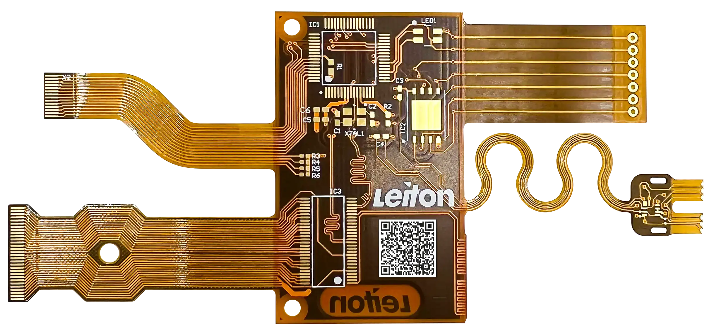
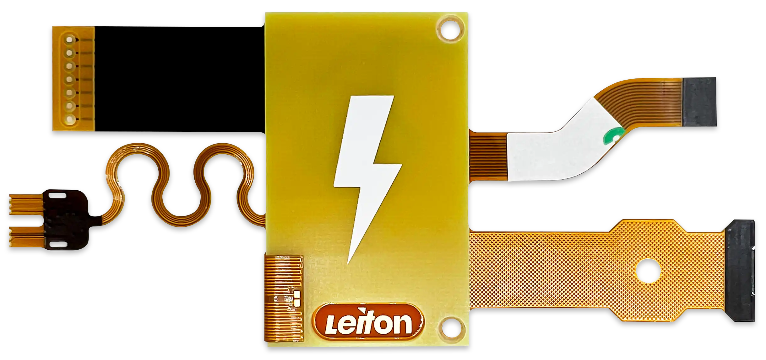
Flex Ideas | FR4 Stiffeners | Shielding Foil | Ultra-Flex Design | Cross-Hatch GND
Flex Design Taken to the Next Level
This sample board shows just how much technology can be integrated into a modern flex circuit. From FR4 stiffeners and shielding foils to ultra-flex areas, special contact solutions, openings, connector gold and adhesive films: discover how mechanical, electrical and manufacturing requirements can be intelligently combined in a very compact space.
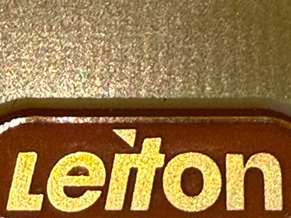
FR4 stiffeners are available in nearly any shape and thickness – silk print is also possible
Stiffeners can be combined with various technologies: Milling, printing, adhesives, etc. Depending on the size, these stiffeners are assembled with high precision automatically, minimizing misalignment and production time. Typical thicknesses range from 0.3 mm to 2.0 mm, with FR4 used for total thicknesses over 0.5 mm.
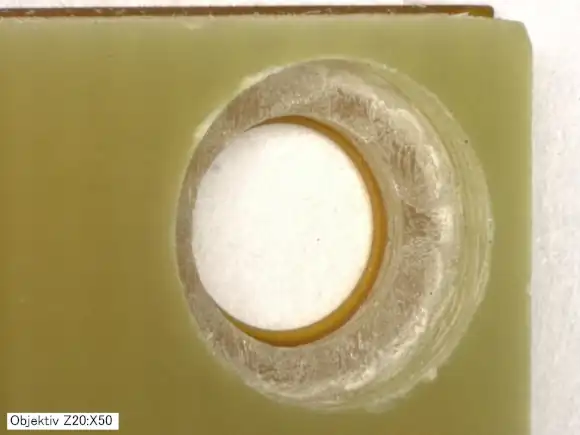
Depth milling or countersink drilling in stiffeners for optimal screwing
Depth milling creates nearly right-angle recesses, while countersunk holes are conical, allowing screws to sit flush. Edge chamfering is also possible to prevent cracking if flexible parts bend over stiff right-angled FR4 edges.
Adhesive shielding foil to protect interference-sensitive areas
Partial shielding foil can be applied to prevent external electromagnetic interference. Placement and shape are flexible, and the foil adapts well due to its flexibility. For double shielding, combining this foil with a copper layer avoids the need for costly 3-layer flexible printed circuits.
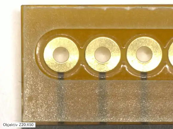
Reinforced THT connector area for stabilization with open solder pads on both sides
Stiffeners are essential for traditional THT connectors to protect solder joints from mechanical stress. Depending on the size and spacing of the solder pads, they can be added in a slot or drilled per pad. It is important that the exposed area is larger than the solder pads.
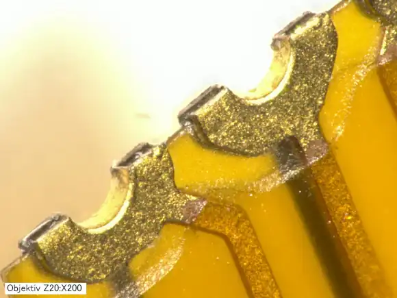
"Half-opens" with partially open vias on the sides
Half-open but fully plated-through sleeves allow precise soldering of wires or other side contacts. Instead of half-open drill holes, additional outline areas can also be plated through, or special plated slots can be placed within the printed circuit.
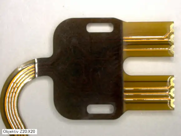
SMD area stiffening for enhanced component stability and quality
SMD component areas also require stiffeners to prevent detachment under bending stress. Even for non-moving areas, thin stiffeners are recommended to reduce risk during installation.
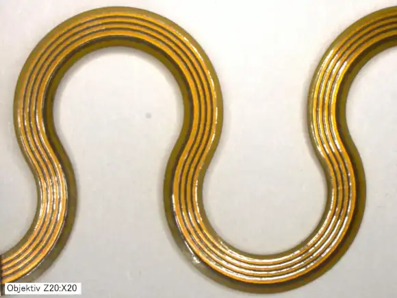
Waveform for ultra-mobile flexibility and stretching in all directions
Flexible "arms" should be designed with snake-like patterns if they need to bend, swivel, and stretch in multiple directions. These designs allow maximum flexibility, but stress is minimized if these areas are kept single-layered. If two layers are necessary, arrange the traces on the top and bottom offset from each other.
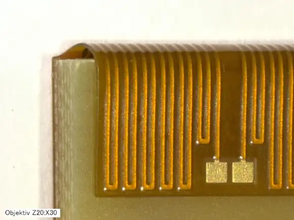
Folded 3M section for economical positioning of components on the FR4 back side
Instead of costly rigid-flex PCBs for a few backside components, these components can be relocated to the bottom side with a "twist". Safety meanders can also be added to prevent unauthorized access to top-side components — the concept of "drill protection."

100% traceability through QR codes with unique ID on each PCB
Increasing traceability requirements for entire assemblies and components can be met with custom QR or barcodes in various formats and sizes. If desired, information like who processed the PCB at Leiton, the testing results, packaging, and more can be tracked.
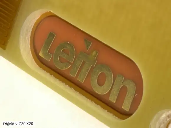
Open areas in FR4 for bottom contact at any position
An alternative to a "smart" bottom connection is to simply separate the double-sided flexible PCB by opening the stiffener. However, these areas should not be too large to prevent mechanical stress on soldered parts. Caution is advised with component placement in recessed areas.
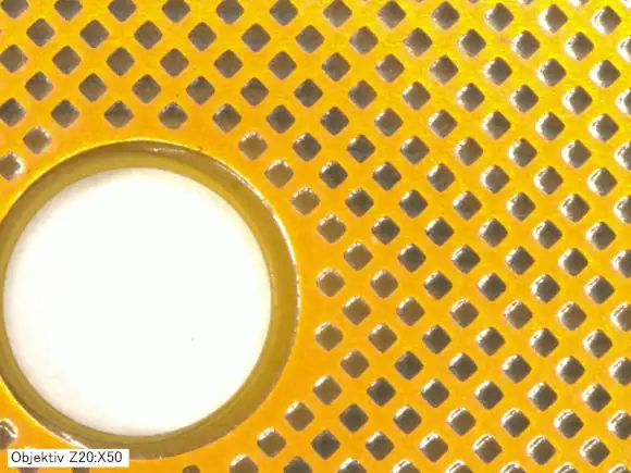
Cross-hatching on the bottom for shielding with minimal movement restriction
Full ground planes on flexible arms significantly reduce flexibility. Therefore, a "cross-hatch" pattern is often an ideal compromise, providing shielding while maintaining some flexibility. Lower material density also reduces the risk of fatigue and cracking.
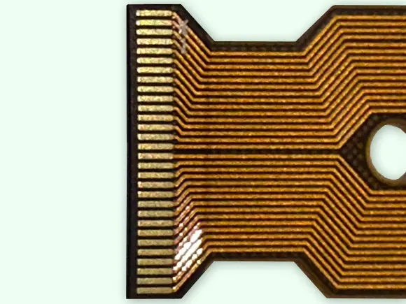
Hard gold thickness of 0.5 to 1.0 µm for increased durability in connection cycles
Partial electrolytic gold can be applied to connectors or within the PCB. When cobalt-doped, this type of gold surface is significantly more durable. The reverse etching process can also be used, where galvanic connections are chemically removed entirely.
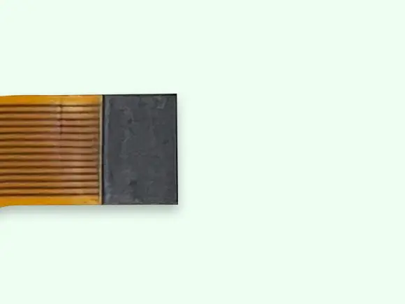
Precise overall thicknesses for zero-insertion force / low-force connectors
The standard thickness for ZIF/LIF connector areas is 0.3 mm. For areas from 0.2 to 0.4 mm, a corresponding polyimide film is used to achieve the exact required thickness. Thicker stiffeners are made with FR4, and stainless steel stiffeners are increasingly used for their thinness, strength, shielding, and durability.
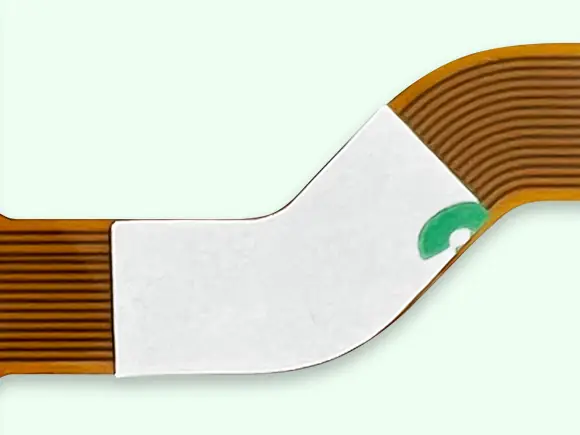
3M double-sided adhesive film for versatile, permanent placement by sticking
3M adhesive films can be applied in any shape and placed on rigid or flexible areas. They are high-temperature resistant for reflow soldering processes and come with an easily removable protective film (liner), allowing for flexible application. The thickness of the 3M film is 50 µm, which should be added to the total thickness.

Elektronik-Design
- Expertise through active exchange
- Expertise through training and further education

- ISO 9001:2015 Quality Management
- ISO 14001:2015 Environmental Management

- UL for rigid FR4 PCBs
- UL for flexible circuit boards
- UL for aluminum IMS boards


