PCB Assembly | PCBA | services | manufacturer | prototype
PCB assembly (PCBA) – THT & SMD assembly of circuit boards

We provide EMS manufacturing for assembled SMT/THT and hybrid printed circuit boards, from express prototypes to production runs - all under one roof. Upon request, we can optimize, test, program, and document everything related to your assemblies. As a professional EMS provider, Leiton offers three options for assembled PCBs:
Express Assembly is available starting from 10 working days or faster, including PCB fabrication and sourcing of all components Made in Germany. Critical components can also be provided by the customer. Due to the extremely high speed and top priority given to these projects, express surcharges of 100% or more are often applicable. In return, you will receive the best service imaginable!
Small Series Assembly is carried out with less urgency, focusing on list prices, component availability, and cost reduction potential. Manufacturing is also done Made in Germany. Lead times typically range from 5 weeks and up. Quality and cost reduction are the primary objectives here.
Large series are produced in a highly cost-optimized manner in our own facility in China. Lead times usually start at 3 months, although prototype production for approval can be completed much faster. Everything undergoes AOI (Automated Optical Inspection) testing and can be delivered with In-Circuit Testing (ICT) upon request. Extensive additional services are available here as well, such as custom enclosures, stamping and bending parts, membrane keypads, injection molding, shelf-ready packaging, device assembly, and more. If desired, the assemblies can be provided with individual (machine-readable) labels for identification and traceability through every step of production. The assembly series are manufactured at Leiton Electronics in Zhongshan, China.


Options |
|---|
| Components | BGA, CSP, LGA, QFN, SOT etc. |
| Smallest component | 0201 |
| Smallest pitch | 150 µm |
| Placement accuracy | +/-40µm |
| Maximum PCB size | 330 x 1200 mm² |
| Maximum PCB thickness | 5 mm |
| Minimum PCB/FPC thickness | 25 µm (Flex FPC) |
| Speed | up to 23.000 components / hour (per SMT line) |
| Feeder capacity | 160 per line (2 SMT machines per line) |
| Maximum component height | 33,5 mm (automatic assembly) |
| Protective coating | Peters LS1307 (standard) |
| Bonding | 25 µm aluminum wire |
| Pressfit | yes, several types |
Assembly of printed circuit boards - fast & professional

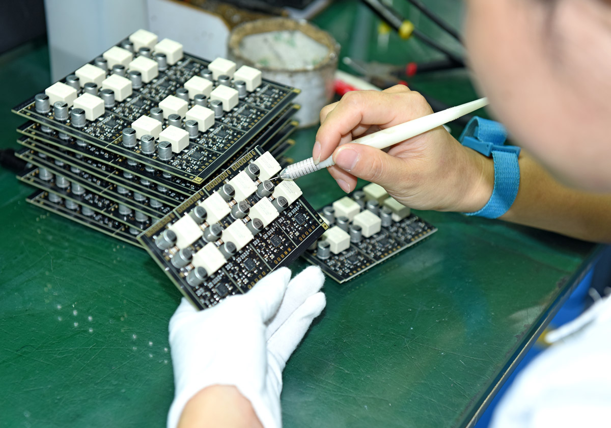
Our Printed Circuit Board Assembly (PCBA) offers the complex manufacturing of electronic devices through the targeted integration of various components onto your circuit board.
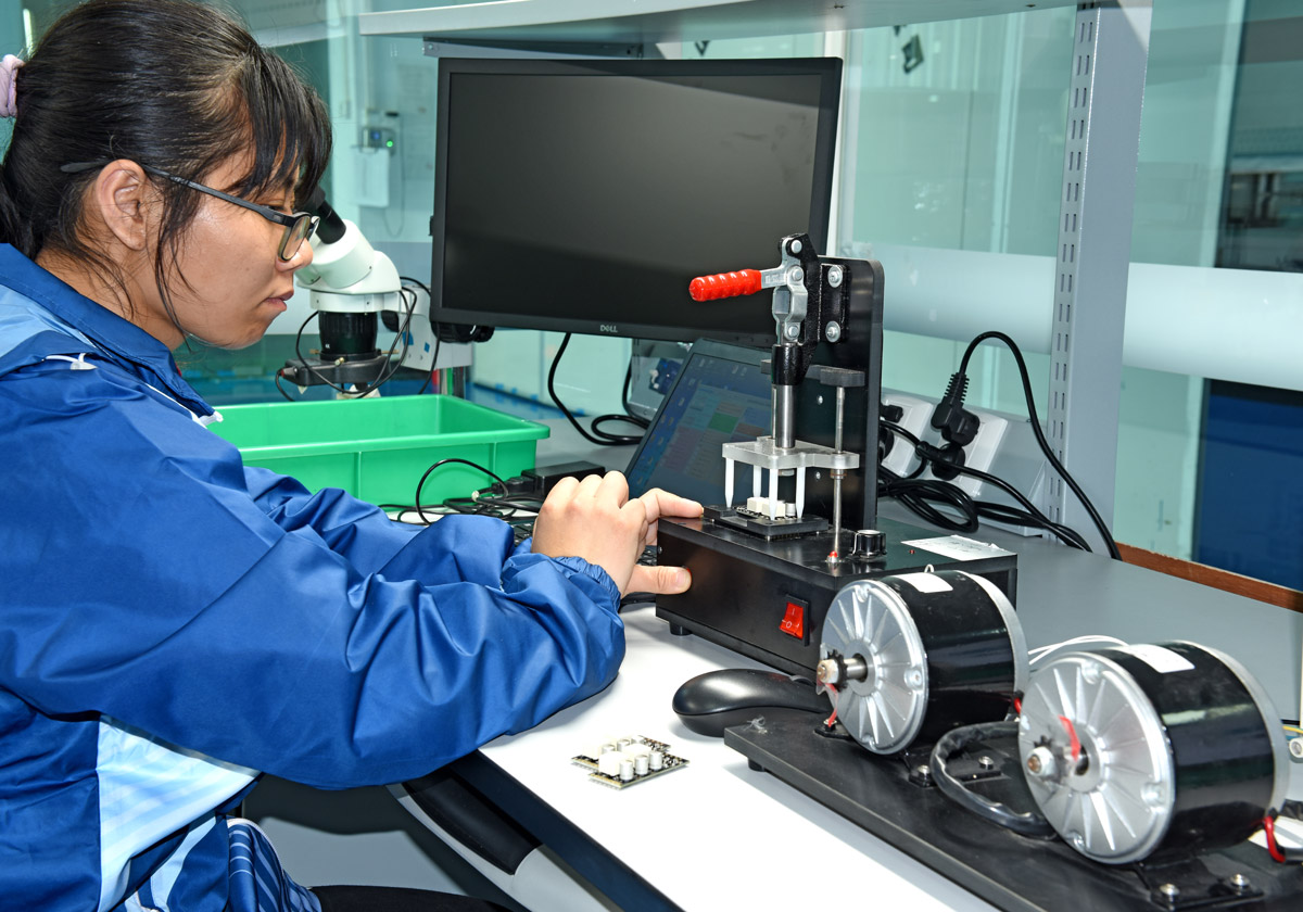
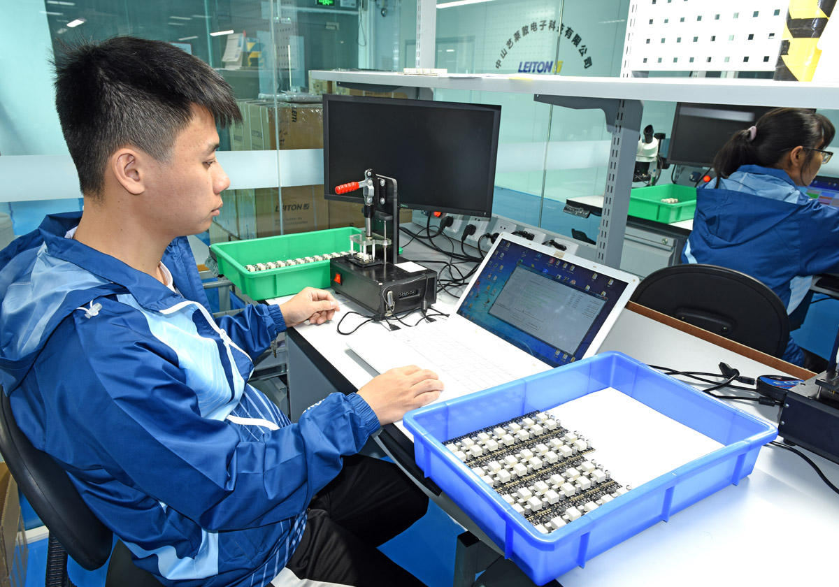
JUKI chip shooters precisely place components such as resistors, capacitors, and microchips under controlled conditions to transform your planned assemblies into functioning systems. We are happy to conduct 100% functional testing on the assembled assemblies according to your testing specifications. Our development engineers design corresponding test adapters and programs for this purpose, optionally with IDs and log files for 100% traceability.
This is why you should have your PCBs assembled by a professional
Engaging a professional EMS (Electronic Manufacturing Services) company like Leiton for the assembly of your printed circuit boards instead of soldering them yourself offers numerous advantages:
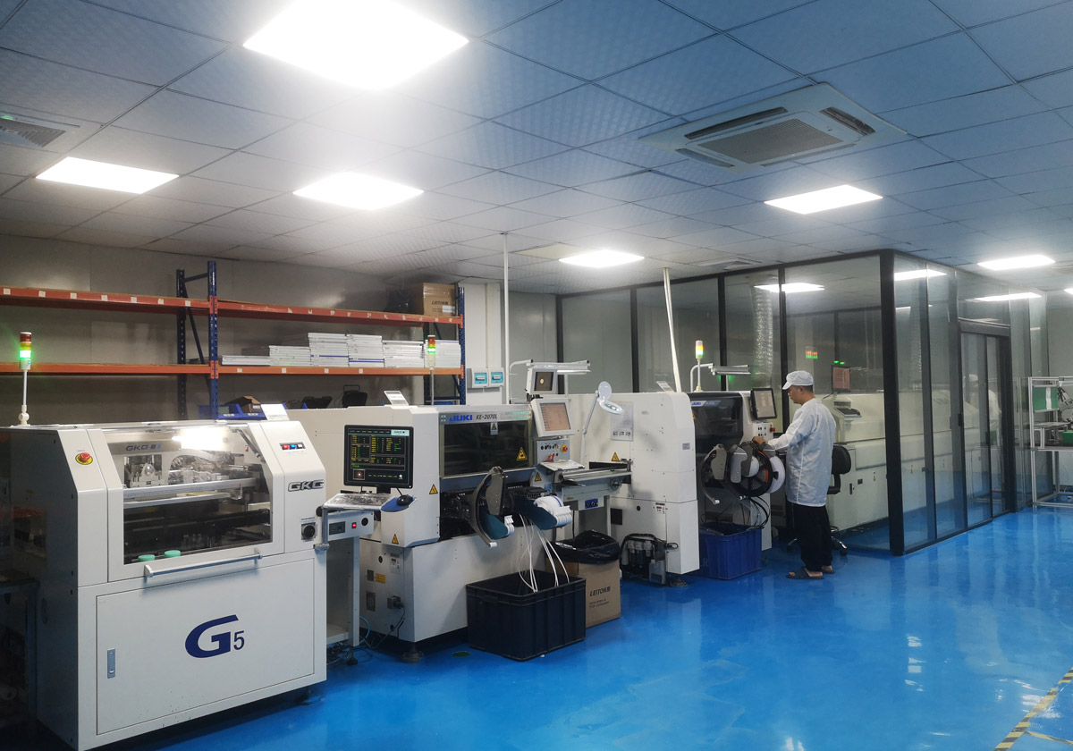
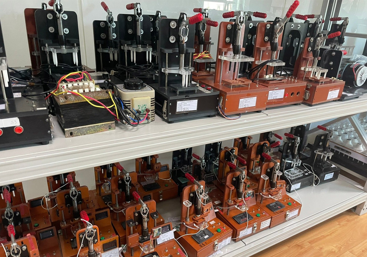
Leiton Electronics machines include:
- Multiple JUKI SMT lines
- Automatic solder paste printers (GKG G5)
- 10-chamber reflow ovens with loading and unloading systems
- AOI systems and burn-in cabinets
- Automatic conformal coating machines
- Keyence microscopes VHX-900F with lenses VH-Z100R/Z100T and extensive measurement and testing equipment
Furthermore, we offer label IDs with scanning at critical process stages, allowing the assembly to be precisely traced back to production even years later. This results in outstanding quality for your printed circuit boards and minimizes potential sources of errors.
Especially with complex boards like Flex, there are significant challenges in assembly that entail a high level of effort. By collaborating with Leiton, you benefit from:
- Automated assembly and testing processes
- Expertise in tooling and fixture construction (Flex-Fixtures)
- Strong supplier relationships with distributors and component brokers
- Additional services: cable harnessing, stamping and bending parts, injection molding, custom packaging, and more
- Traceability via ID/QR code
All of these lead to increased production speed and reliability. Your overall lead times are significantly reduced, and your assemblies can be made operational more quickly. Additionally, costs for acquiring and maintaining assembly equipment and training your own staff are eliminated.
component procurement, and assembly testing. We can advise you on the selection of suitable components, materials, and processes to ensure that your PCBs meet the specific requirements of your project. If you don't have a test description for your assembly, we can work together to develop one.
- Component Procurement: Leiton assists in sourcing the necessary components for your PCB assembly, ensuring the availability of quality components for your project.
- Component Selection Guidance: Leiton offers expertise in helping you choose the most suitable components for your PCBs, considering factors such as performance, price and availability.
- Assembly Testing: Leiton provides testing services to verify the functionality and reliability of your assembled PCBs, ensuring they meet quality your defined standards.
- Test Description Development: If you lack a test description for your assembly, Leiton collaborates with you to develop one.
Various types of calibrations are possible. Here's an overview:
- IC Programming: Writing software code for microcontrollers, microprocessors, and other types of ICs.
- EEPROM/EPROM Flashing: Flashing EEPROMs (Electrically Erasable Programmable Read-Only Memory) and EPROMs (Erasable Programmable Read-Only Memory) memory chips.
- Software Programming: Software development for embedded systems, firmware, and ICs.
- PLD (Programmable Logic Devices) Programming: Programming PLDs, like FPGAs (Field-Programmable Gate Arrays).
- Calibration Services: Fine-tuning electronic devices or sensors, including various types of calibration services such as temperature calibration, voltage calibration, or sensor calibration.
each assembled PCB complies with the specified standards:
- IPC-A-610: This is the industry-recognized standard for acceptance criteria of soldered electronic assemblies. It establishes visual requirements for the quality of solder connections, components, and assembly processes.
- IPC-J-STD-001: This standard contains requirements for soldering electronic assemblies and serves as a reference for process control, materials, and testing in the soldering process.
Regardless of the underlying standards, assembly is carried out with extensive testing:
- Functional tests: Verifying that the assembly meets the expected functions. We are happy to accommodate even the most comprehensive testing requirements.
- Electrical tests: Measuring electrical parameters and checking performance parameters within the assembly.
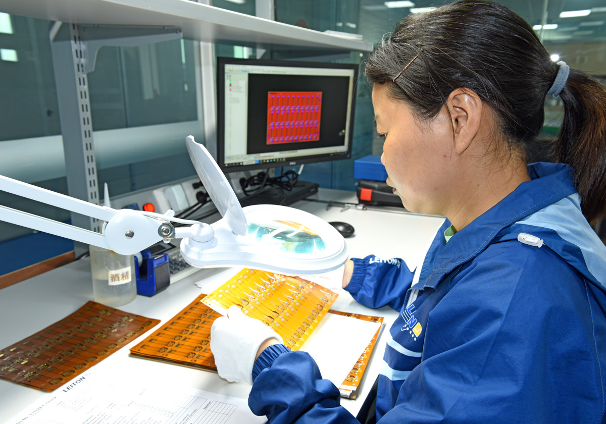
- Bare PCB E-test: Each PCB is 100% electrically tested before assembly, as a mandatory step.
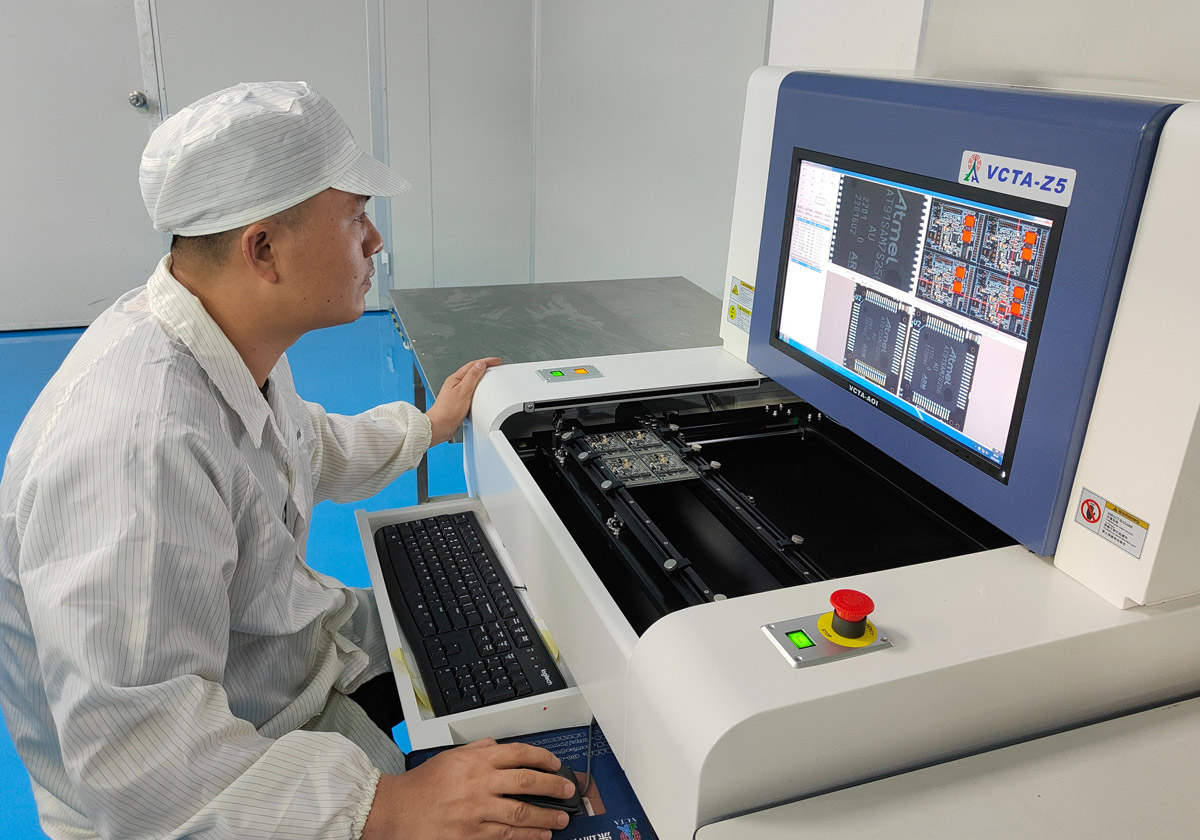
- Visual inspection: Checking the assembly for external defects, incomplete solder connections, and deviations from the design, either manually or through AOI (Automatic Optical Inspection), depending on complexity.
- Mechanical tests: Testing mechanical stability, resistance to vibration, and shocks.
- Environmental tests: Exposing the assembly to extreme temperatures, humidity, vibration, or other environmental conditions to test its reliability (e.g., climate chamber).
By collaborating with Leiton, you receive high-quality, tested PCBs and benefit from time and cost savings, as well as the expertise and experience of our team. This allows you to focus on your core competencies such as development and marketing while simultaneously achieving optimal manufacturing results through us.
Why order assemblies from Leiton?
PCB assembly: SMD production
Surface Mount Technology (SMT) ist ein moderner Ansatz zur Bestückung von Leiterplatten mit elektronischen Surface Mount Device (SMD) Bauteilen. Im Gegensatz zur herkömmlichen Through-Hole-Technologie, bei der Bauteile durch Bohrungen gesteckt und auf der Rückseite der Leiterplatte gelötet werden, werden bei der SMT-Fertigung die Bauteile direkt auf der Oberfläche der Leiterplatte platziert und dort verlötet. Dies bietet eine Reihe von Vorteilen, darunter:
- Space savings: Due to the smaller size of SMD components and the ability to place them more densely, more compact and higher-performance assemblies and devices can be produced.
- Higher production speed: Automated pick-and-place assembly combined with reflow soldering enables faster and more efficient manufacturing compared to THT.
- Improved high-frequency performance: SMT technology reduces parasitic effects and allows for superior high-frequency characteristics in electronic circuits.
- Cost reduction:: Although initial investments in SMT equipment are higher, automated production, reduced material usage, and shorter production cycles can lead to long-term cost savings.
PCB assembly: THT production
THT stands for "Through-Hole Technology," known as "Durchsteckmontagetechnik" in German. This is a traditional approach to manufacturing electronic assemblies, where components are inserted through holes in the circuit board and soldered on the backside of the board. THT manufacturing was widely used in the early days of the electronics industry before the development of Surface Mount Technology (SMT).
Although SMT manufacturing predominates in many areas today, THT manufacturing still has its applications and advantages:
- Greater durability: THT components often have more robust connections and are better suited for applications subject to vibrations, shocks, or heavy mechanical stress.
- Easy manual repairs: THT connections can be soldered or desoldered by hand more easily, facilitating the repair of assemblies.
- Higher electrical tolerance: THT connections are often better suited for applications with high voltages or currents.
THT manufacturing is frequently used in industries such as aerospace, defense, automotive, and other high-reliability applications where the robustness of connections and the possibility of manual repairs are important.
Leiton GmbH – Customized PCBs & professional assembly
From SMD (Surface Mount Device) to THT (Through-Hole Technology) to manual assembly, we offer tailored solutions for your electronic assemblies. Starting from 1 piece in express mode to production runs with call-off inventory, from simple populated circuit boards to fully function-tested electronic products with custom enclosures and packaging. We provide consultation from layout creation to the finished assembly.
Printed circuit boards are equipped with electronic components through a process known as "assembly." There are two primary methods for placing components on PCBs: Surface Mount Technology (SMT) and Through-Hole Technology (THT).
SMT Assembly (Surface Mount Technology):
In SMT assembly, components are placed directly on the surface of the PCB. This process is typically automated using specialized machines. The steps of the SMT assembly process are as follows:
- PCB Preparation: The PCB is prepared by cleaning and coating it with solder paste. The solder paste contains tiny solder balls and is applied to the locations where the components will be attached.
- Component Placement: Automated assembly machines precisely place SMD components on predetermined positions on the PCB. These machines can often place tens of thousands of components per hour from reels or trays onto the PCB, depending on component size and arrangement.
- Reflow Soldering: The PCB with the placed components is conveyed into a reflow soldering oven. The oven heats the solder paste to melt the solder, attaching the components to the PCB. Reflow ovens often have a conveyor belt and multiple chambers (6-12 chambers) with different temperatures where the assembled assembly goes through various stages (preheat, peak temperature/soldering, cooling).
- Inspection and Testing: The assembled and soldered PCB is inspected for defects, solder joints, and quality issues. This can be done using automated inspection machines (AOI) or visual inspection. Such inspection can be done "in-line," meaning directly in the assembly process, or it can be performed separately at a dedicated workstation.
THT Assembly (Through-Hole Technology):
In THT assembly, components are inserted through holes in the PCB and soldered on the backside of the PCB. Here are the steps of the THT assembly process:
- PCB Preparation: The PCB is prepared by creating holes at the locations where THT components will be inserted. For more stable connections, double-sided PCBs are recommended, even if the layout initially requires only a single layer.
- Component Placement: Components are manually or with the assistance of automated insertion machines placed on the PCB. The components are positioned so that their pins go through the holes in the PCB.
- Soldering: The PCB with the inserted components is soldered using wave soldering or manual soldering. In wave soldering, the PCB is passed over a wave of molten solder, allowing the liquid solder to rise through the holes and form connections once it cools.
- Inspection and Testing: Similar to SMT assembly, the assembled and soldered PCB is inspected for defects, solder joints, and quality issues.
The selection of the appropriate assembly method depends on factors such as component size, application, production volume, and other technical requirements.
Printed circuit boards can also be assembled manually depending on their complexity. If you have limited experience with manual assembly and only possess a soldering iron, it's advisable to use Through-Hole Technology (THT) components. These are components designed for "through-hole" insertion, and they can be relatively easily placed in their respective component holes and soldered individually.
Things get a bit more complicated when dealing with Surface Mount Device (SMD) components. These are components that are placed on pads without going through holes, and soldering them individually with a soldering iron can be very challenging. Usually, SMD components require the application of solder paste to the pads. This can be done selectively and cautiously, or you can obtain a tool called a solder paste stencil, which allows for the professional "squeegeeing" of solder paste onto all the pads. Subsequently, you'll need an oven capable of reaching the melting point of the solder paste, which is around 220°C. In principle, this can also be done with some conventional ovens, but we strongly advise against using an oven that is used for food preparation due to the potential release of fumes. It's important to note that self-soldering may expose both the components and the assembly to prolonged heat in this temperature range, which can be detrimental. Therefore, professionals use reflow ovens that don't stay at the melting point for long but provide a short temperature spike above it (typically a few seconds at around 260°C). This ensures that the solder flows while the high temperature is applied only briefly. Achieving this with conventional ovens can be challenging.
If manual assembly seems too complicated or if you lack the necessary equipment, feel free to inquire with us about assembling your assemblies.
SMD assembly, a part of Surface Mount Technology (SMT), automates the placement of tiny components on printed circuit boards. This process begins with PCB preparation, including cleaning and solder paste coating for precise component placement. SMD stands for the type of component used, which lacks "legs," and is referred to as "Surface Mount Devices" or "SMDs."
The typical sequence of SMD assembly is as follows:
- PCB Preparation
Cleaning and Coating: The PCB is prepared by undergoing cleaning and being covered with a layer of solder paste. This paste contains microscopic solder balls and is applied to the locations where the components are to be attached. This is usually done using a solder paste stencil (LINK TO STENCIL SHOP). - Component Placement
Automated Placement: Specialized machines precisely position SMD components at the predetermined locations on the PCB. The accuracy in this process can often be as fine as +/-30 µm. Depending on the size and arrangement of the components, these machines can often place thousands per hour from reels or rolls onto the PCB. - Reflow Soldering
Reflow Soldering Process: The PCB with the placed components passes through a reflow soldering oven. During this process, the solder paste is heated to melt the solder, creating a connection between the components and the PCB. Reflow ovens are typically equipped with a conveyor belt and multiple chambers (6-12 chambers) with different temperatures. This allows the assembly to go through various phases, including preheating, peak temperature/soldering, and cooling. - Inspection and Quality Control
Component Inspection: The assembled and soldered PCB undergoes inspection to identify defects, solder joints, and quality issues. This can be done using automated inspection machines (AOI) or visual inspection. Inspection can either be conducted "in-line" during the assembly process or later at a dedicated workstation separately.
THT assembly ("Through Hole Technology") refers to the placement of components by inserting them through holes in the printed circuit board. After insertion, the components are soldered in place. Here are the steps of the THT assembly process:
- PCB Preparation
Drilling Preparation: PCBs are prepared for THT components by creating holes at the respective positions. Through-hole plated boards enhance stability, even in the case of simple layouts. - Component Placement
Manual or Automated Placement: Components are placed manually or with the help of machines so that the pins go through the holes in the PCB. - Soldering Process
Wave Soldering or Manual Soldering: The PCB with components is subjected to wave soldering or soldered manually using a soldering iron. Wave soldering uses a solder wave to pass through the holes, creating connections. - Inspection and Quality Testing
Component Inspection: Similar to SMT assembly, the soldered boards are monitored for defects and quality issues.
The choice of assembly method depends on factors such as component size, application, production volume, and technical requirements.
SMT (Surface Mount Technology) and THT (Through-Hole Technology) each have their advantages and disadvantages:
SMT Assembly (Advantages):
- Space Saving: Smaller components and reduced board space allow for more compact designs.
- Higher Speed: Automated SMT assembly is faster because machines can place many components simultaneously.
- Better High-Frequency Properties: SMT offers lower parasitic effects and is advantageous for high-frequency circuits.
SMT Assembly (Disadvantages):
- Repair Complexity: SMD components are more challenging to repair or replace as they are smaller and require specialized tools.
- Sensitivity: SMD components can be sensitive to mechanical stress, making handling and transportation more demanding.
THT Assembly (Advantages):
- Mechanical Stability: THT connections are more robust and resistant to vibrations and mechanical stress.
- Easier Repairs: THT components are easier to replace or repair as they have larger pins and holes.
- Versatility: THT is well-suited for high-current or high-power applications.
THT Assembly (Disadvantages):
- Larger Components: THT requires more board space, which can lead to larger and heavier designs.
- Lower Speed: Manual placement of THT components is slower and requires more labor.
- Poorer High-Frequency Properties: THT may exhibit higher parasitic effects and is less suitable for high-frequency circuits.
The choice between SMT and THT depends on the specific project requirements, including component size, design complexity, production volume, and desired electrical properties. Often, a combination of both methods is used to leverage the advantages of each approach.
The two abbreviations "SMD" and "SMT" refer to the same technology, which involves electronic components being placed on pads and not inserted through holes.
SMD = Surface Mount Device
SMT = Surface Mount Technology
So, SMD refers to the component itself ("Device"), while SMT refers to the technology in general. Often, SMT and SMD are used interchangeably, for example, when talking about "SMD assembly" or "SMT assembly." Both terms describe the same process; one specifies "what" is being assembled (SMD), and the other specifies "how" (SMT).
Printed circuit boards are populated with a variety of electronic components. These components can be broadly categorized into different types. Here's an overview of the categories along with the typical package types of components:
- Active Components:
- Integrated Circuits (ICs): SMD, DIP, QFP, BGA.
- Transistors: SMD, TO-92, SOT-23.
- Operational Amplifiers: SMD, DIP.
- Voltage Regulators: SMD, TO-220.
- Microcontrollers: SMD, QFP, BGA.
- Passive Components:
- Resistors: SMD 0201, 0402, 0805.
- Capacitors: SMD 0603, 0805, 1206.
- Inductors/Coils: SMD, Axial, Radial.
- Crystals: SMD, HC-49.
- Electromechanical Components:
- Connectors: Pin headers, socket headers, board-to-board, ZIF/LIF.
- Switches: Tactile switches, toggle switches, slide switches.
- Relays: SMD, PCB, Reed relays.
- Potentiometers: SMD, Through-hole.
- Optoelectronic Components:
- Light Emitting Diodes (LEDs): SMD, Through-hole.
- Photodiodes: SMD, Through-hole.
- Optocouplers: SMD, Through-hole.
These component categories are placed and soldered onto printed circuit boards based on application requirements to form electronic circuits.
Mixed assembly, also referred to as mixed technology or mixed mounting, pertains to populating a printed circuit board with both surface mount devices (SMD) and through-hole technology (THT) components on the same board.
In mixed assembly, electronic components with different technologies can be combined to leverage the advantages of both approaches. For example, SMD components can be used for compact designs, higher speeds, and better high-frequency characteristics, while THT components can be employed for robust connections and high-current applications.
Mixed assembly requires specialized knowledge of manufacturing processes and careful planning of the correct assembly sequence to ensure that the different process steps do not negatively impact each other.
BGA assembly stands for "Ball Grid Array" assembly and refers to a specific type of surface mount of integrated circuits (ICs) on printed circuit boards. In BGAs, the IC connections are arranged in the form of small balls in a grid pattern beneath the component.
BGA assembly offers several advantages, including:
- High connection density: The close arrangement of solder balls beneath the component allows for more connections to be accommodated in a smaller area, resulting in higher packing density.
- Effective heat dissipation: The multitude of connections enables better heat dissipation from the IC component, which is crucial for high-performance components.
- Reliable connections: The solder balls provide robust and reliable electrical connections that are less susceptible to short circuits or poor solder joints.
- Enhanced performance: BGAs can handle high-speed applications since shorter connection paths improve signal integrity.
However, BGA assembly requires special manufacturing processes because the solder balls are not directly visible. Quality control of the solder joints may necessitate the use of X-ray equipment.
BGA assembly is commonly used in demanding applications such as computer processors, graphics chips, microcontrollers, and other highly integrated circuits that require high performance and reliability.
Press-fit process refers to the insertion of electronic components into plated-through holes on a printed circuit board (PCB) instead of attaching them through soldering. This is often applied to components that, due to their size, shape, or electrical properties, cannot be easily soldered to the surface of the PCB. The requirements for hole tolerances are usually higher for press-fit components than for soldered components. Therefore, it is essential that the press-fit requirement is specified to the PCB manufacturer along with the datasheet of the press-fit component being used. Only in this way can it be ensured that the press-fit components will have optimal retention in the PCB.


