


Special options, larger quantities, or faster delivery times available in the online calculator or on request.


Leiton GmbH | Printed circuit board | PCB | manufacturer | Germany | order | online
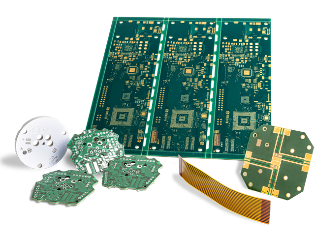
Leiton GmbH – Printed circuit board (PCB) manufacturer from Germany
Leiton Circuit Boards & Assembly - Count on the Best Service! Prefer working with small numbers? Then you're in the right place. We offer a wide range of circuit board technologies and assembly options from Germany and Asia, all in the highest industry quality at fair prices. Convince yourself on our website, contact us, or visit us anytime.
And don't forget: instant pricing available anytime through our online calculation!
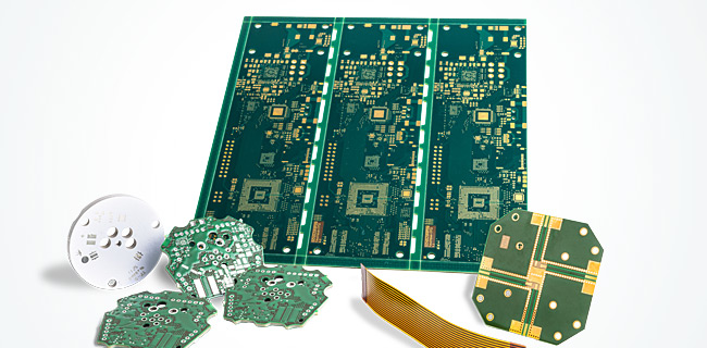
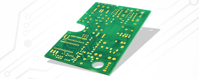
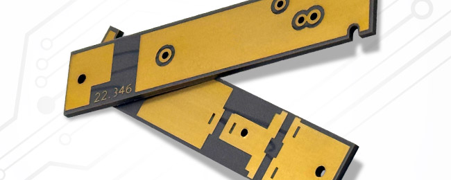
Circuit boards come in a range of types, from express prototypes to production series, assembled or unassembled. Here's a brief overview of our offerings.
Important: many types are available for online calculation!


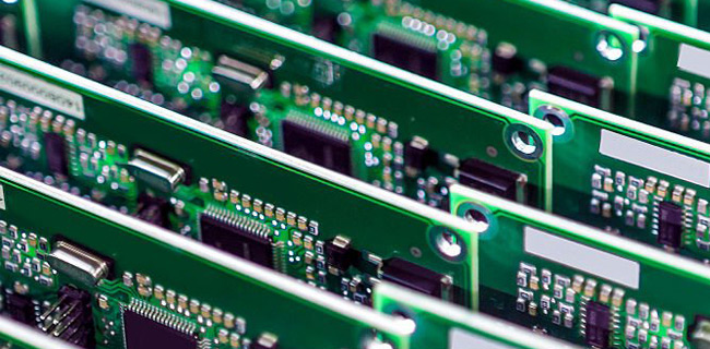
Your circuit boards are always manufactured in the highest industry quality, compliant with RoHS and REACH regulations. We offer express service as well as various options for batch and call-off orders for series production. Electrical testing is included, and for assemblies, we provide individual functional testing.
PCB Series can be manufactured beyond mere assembly with custom injection-molded enclosures, cables, and stamped-bent parts. We can even provide individual packaging in your company's design. Configure your circuit boards quickly and conveniently in our online calculation or send us your data via email or through our contact form. For complex circuit boards, you can also upload your data with the specifications through the inquiry form.
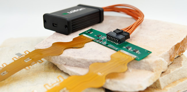
If you are interested in fully assembled assemblies, please upload the circuit board design along with a bill of materials (Excel-BOM) here. We assemble prototypes with express service, as well as fully tested series quantities. Series production can include custom injection-molded enclosures, cables, and stamped-bent parts beyond just assembly.


If you have any further questions about our PCBs or our service, please feel free to take a look at our FAQ overview. Here you can find many more helpful information.
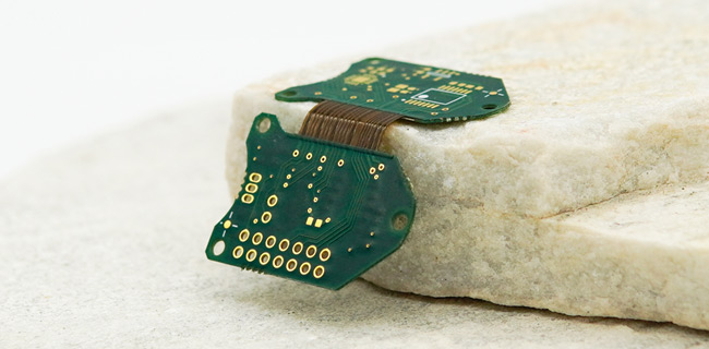
Leiton offers rigid, flexible, rigid-flex, and IMS circuit boards, available for online calculation or upon individual request. Here's an overview of the types of circuit boards:
All circuit boards at Leiton are individually manufactured according to ISO9001 industry quality standards. The provided data is carefully reviewed by our CAM engineers for feasibility, manufacturability, and completeness before production. Any inquiries or clarifications are handled personally and individually by our German colleagues to ensure that the first delivery meets the desired outcome immediately.
At Leiton, various variants can be ordered online. However, for any technology, the option to place an order via email or the inquiry form is also available. At Leiton, there is no distinction in pricing between whether you calculate and order online yourself or send us the data via email.
Here is a list of available countries for PCB delivery along with their respective shipping options and costs:
Leiton has a network of highly specialized PCB manufacturers in Germany, Europe, and Asia. Depending on the technology, delivery time, quantity, and required certifications or special options, the optimal supplier for your circuit board project is selected. This allows you to save time-consuming inquiries with multiple manufacturers by obtaining everything from one source.
Leiton offers very competitive entry prices for circuit boards through the "sharing" concept. In this approach, circuit boards are combined with other orders, allowing everyone to save on setup costs. Overall, Leiton positions itself as a mid-range provider in terms of pricing, offering fair prices for high quality, above-average reliability, and personalized consultation with individualized service.
Leiton generally delivers on invoice (payment term of 14 days, without deductions). In the online calculation, payments via PayPal or credit card (VISA, Mastercard) are also possible. Individual payment terms are, of course, available upon individual agreement.
The manufacturing time for circuit boards depends on the technology and quantity. Simple prototypes can be produced and shipped within 2 working days. However, even for series production, Leiton can expedite the process, and the boards can be manufactured in just a few working days (5-8 WD). For series production, Leiton also offers split orders. With split orders, blanks are not produced at different speeds, but are shipped using different means of transportation: partial delivery by air freight, while the rest is shipped by sea, for example. This approach helps save costs, and you receive a single mixed price with the actual urgently needed quantities in advance.
Yes, Leiton can produce 1- and 2-layer PCB prototypes in as little as 2 working days. Multilayers starting from 4 layers are offered with a 3 working day express service. Medium-sized series up to 2.5m² can be available in as little as 5 working days, but even series up to 50m² or more can be manufactured with an express service. As for assembled circuit boards (PCBA), they are also available with an express service starting from 5 working days. Simply contact us regarding your desired timeframe, and we will offer you the fastest possible delivery time.
At Leiton, you benefit from the advantages offered by component distributors, such as a wide range of technologies and availability from small quantities to large volumes. However, Leiton goes beyond that by providing personalized and individual engineering consultation, as well as tailored logistics and delivery solutions, including call-off stock and framework agreements. Technical clarifications and CAM data processing are handled by Leiton, while PCB manufacturing is carried out within a large network of carefully selected manufacturers. This allows for seamless transfers within the network in case of changing requirements or quantities.

Elektronik-Design
- Expertise through active exchange
- Expertise through training and further education
- ISO 9001:2015 Quality Management
- ISO 14001:2015 Environmental Management

- UL for rigid FR4 PCBs
- UL for flexible circuit boards
- UL for aluminum IMS boards


