

solder fingers
Edge connectors | Polyimide core | solderable fingers | flexible circuit board | optionally formed
Polyimide-cored solderable fingers instead of a connector, optionally permanently formed
Edge connectors with polyimide core are polyimide-supported, solderable fingers that replace a separate connector – straight or optionally permanently bent into shape. Technically, these are copper fingers that extend beyond the outline of the flexible circuit board. They are exposed there from the coverlay, solderably tinned or gold-plated. This creates the connection from the circuit board itself, without a separate connector. A continuous polyimide core supports the exposed fingers. This distinguishes the solution from classic Sculptured Flex, where the fingers consist of solid copper and are unsupported, bare-metal exposed, without polyimide in the finger. The polyimide support makes the structure more robust at the bending root and significantly cheaper to manufacture.
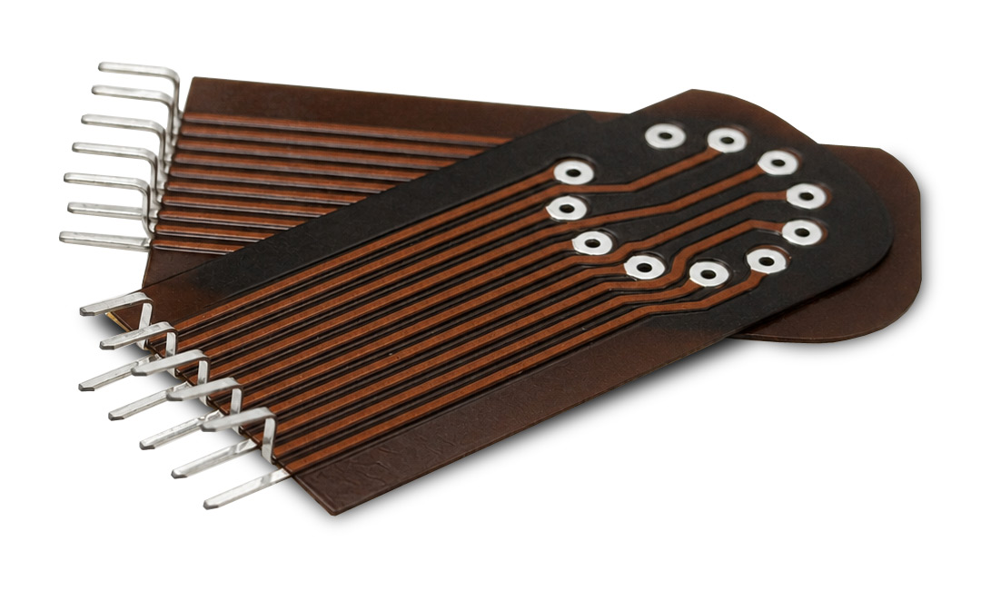
Straight fingers are suited to direct soldering onto a mating surface or to plugging into a socket. If the fingers are formed, the shape is not tied to a single function. Depending on tool and geometry, the formed finger acts as a bridge, as a connection between two PCBs, as a link across several levels or to contact offset assemblies. Unlike a pluggable card-edge contact, the edge-board contact, the finger is soldered and holds permanently rather than merely being plugged in.
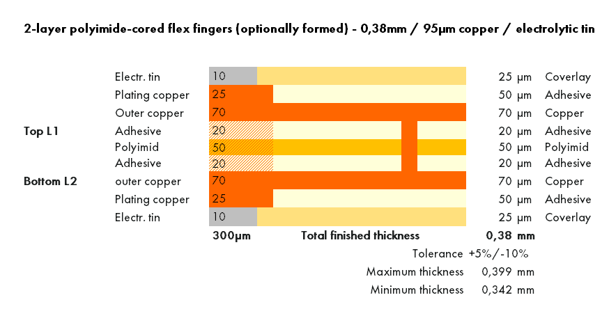
The exposed fingers are more mechanically sensitive than ordinary component leads and must be handled with care before and after bending. The differing copper thickness is created by conventional copper plating in the contact area, not by costly differential etching, which on sculptured flex often removes more than 90% of the copper. The base copper is typically 70 µm, so that the exposed fingers are selectively plated up to over 100 µm. ENIG is possible as a final finish. However, if the fingers are subsequently formed, electrolytic tinning (about 10 µm) is preferable.
Electrolytic tin bends better and is not as brittle as the nickel beneath a gold finish. If the formed variant is chosen, a customer-specific bending tool is also required, so one-off setup costs apply. The straight variant, with projecting fingers only and no bending, needs no customer-specific tool.
When to use polyimide-cored solder fingers
Polyimide-cored solder fingers are the right choice when solderable connections are needed straight from the flexible PCB. A separate connector can then be omitted. The straight variant suits cases where a flat, solderable connection onto a mating surface or into a socket is sufficient.
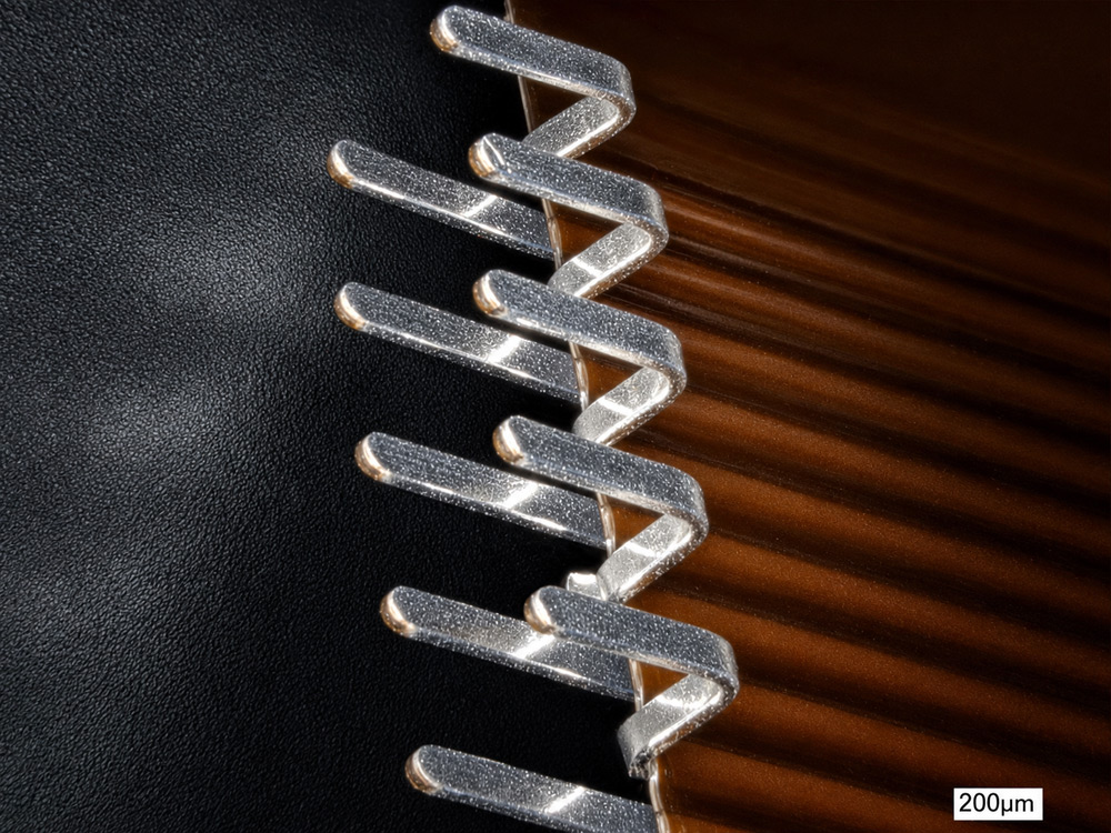
The formed variant suits cases where two PCBs are joined at an angle or with a gap, where several levels are contacted in a tight space, or where height-offset assemblies must be reached. On the example PCB every second finger is formed, as these are inserted like pins into offset holes.
The formed solder fingers used in this application example are shown in Figures 2 and 3.
Applications
Comparison table
Related interconnection techniques compared, with definition, advantages, disadvantages and cost. The Leiton design is called polyimide-cored solder fingers.
| Technique | Definition | Advantages | Disadvantages and cost |
|---|---|---|---|
| Polyimide-cored solder fingers (Leiton) | Solderable copper fingers project from the flexible PCB, supported by a continuous polyimide core. Thickness built by copper plating; straight or permanently formed. | No connector. Supported, robust bend root. Solderable on both sides. Defined shape, repeatability ±3°. Suitable for series. Lower overall cost thanks to a conventional process. | Formed variant needs a customer-specific tool, one-off setup cost. |
| Classic sculptured flex (differential etching, unsupported) | Thick copper is etched down zone by zone, terminal fingers thick, bend zone thin in the polyimide area. The fingers therefore have no polyimide core. | Thick, robust bare contacts and thin flex zones in one part. Pluggable into sockets. High current capability. | Elaborate sequential etching plus laser back-baring. Often removes more than 90% of the copper area. Unsupported fingers are sensitive. High cost. |
| Bump or pedestal plated (differential copper) | Locally heavily plated SMT pads, for direct coupling to other components or PCBs. | Thick, well-solderable pads. Robust contacting. | Only for flat SMT connections, no angled or 3D connections. Process-related variations in height and shape. Medium to high costs. |
| Flying leads / unsupported flex conductors | Coverlay and base film removed, free-standing bare conductors, often by laser, for direct soldering. The term is also used in the market for cable ends. | Connectorless, direct soldering, thin and light. | Free-standing and very sensitive. Laser process is expensive. Confusable with cable. Medium to high cost. |
| Edge-board contact or ZIF/LIF FFC | Detachable plug connection at the board edge, or a flexible PCB in a ZIF/LIF socket (Zero or Low Insertion Force). | Detachable and service-friendly. Tool-free assembly. Low-cost volume connectors. | Needs a socket, often an additional stiffener. Not permanently vibration-proof. Additional part. Connector system adds cost. |
| Discrete jumper or connecting component | A separate part (SMD jumper, bridge jumper, FFC, wire) bridges two points or PCBs. | Standard part, simple, available from stock. | Extra part plus placement plus additional solder joints. More failure sources and logistics. Cost: part plus assembly. |
Advantages
-
Connection from the PCB:
no separate connector, fewer parts and less assembly effort. -
Polyimide-cored fingers:
continuous polyimide core to the tip, robust bend root, cheaper than exposed, unsupported sculptured flex. -
Solderable all round:
the two copper layers are electrically joined via the edge metallisation of the fingers, creating one conductor with copper on both faces and at the edges. Both faces are tinned or gold-plated and solderable on both sides; the parallel layers increase current capacity. -
Defined, repeatable shape:
bend angle even beyond 90° (design-dependent), repeatability ±3°, multiple bends possible with tools offering many degrees of freedom. -
Material build:
base copper usually 70 µm; the exposed polyimide-cored fingers are reinforced by copper plating, for example to 100 µm; recommended finish electrolytic tin about 10 µm. -
Formability:
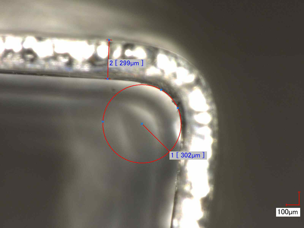
the fingers are formed once and permanently into defined 3D geometries, tight inner radius down to about the material thickness (roughly 1:1), for angled, stepped or bridging connections. The formed contour is retained.
Important notes:
Requires at least a two-layer flex board so that the fingers can be plated up fully and all round. Despite the polyimide core the exposed fingers are mechanically sensitive and should be protected from load during processing. The achievable bend angle and deflection depend on the neighbouring fingers and the geometry of the flexible PCB (FPC, Flexible Printed Circuit). The exposed fingers are reinforced by copper plating and electrolytically tinned. If formed, the tool is customer-specific, with one-off setup costs per geometry. Compliance certificates such as RoHS and REACH are available.
The fingers are designed for soldering. A press fit is critical with the fine fingers and can cause defects; plugging alone without soldering leads to intermittent contacts.
Surface finish
The finish is applied before forming and is bent along with the finger. Therefore not only the ductility of the copper matters but also that of the finish. High strains occur at the outer fibre of a tight bend radius. A thin, brittle coating cracks there and exposes the copper; a thick, ductile coating is stretched along and continues to protect the copper. For the formed fingers electrolytic tin is therefore the right choice. ENIG and immersion tin are options for straight, unformed fingers and flat surfaces.
| Finish | Suitable for formed fingers | Advantages | Disadvantages | Application |
|---|---|---|---|---|
| Electrolytic tin, about 10 µm | suitable | Very ductile, about 50% elongation. Stretched along during bending, all-round copper protection, well solderable. | Limited solderability shelf life, about 6 to 12 months. Possible whiskers, reduced by matte tin. | Permanently formed fingers |
| Immersion tin, about 1 µm | unformed only | Very flat, fine structures, good for single soldering. | Very thin, high proportion of brittle copper-tin phase, cracks on bending. Short shelf life. | Flat surfaces, straight fingers |
| ENIG, electroless nickel plus immersion gold | unformed only | Flat, well solderable, good shelf life, wire-bondable. | Brittle nickel cracks on bending, the crack runs into the copper. More expensive. | Straight fingers, flat contact areas |
Request a quote
For a sound quotation for polyimide-cored solder fingers, a few details are enough:
- Layout data (ODB++, Extended Gerber, KiCAD or similar)
- Geometry and target shape of the fingers
- Desired bend angle
- Copper thickness in the flex area and at the fingers
- Surface finish
- Quantity and any deadlines
A sketch or drawing of the bend is ideal.
The bending tool, CAM inspection and series production come from us. For edge connectors with polyimide core, we support projects from the initial feasibility check through prototypes and into series production. Prototypes and samples are manufactured in Germany; series production runs from Germany or Asia depending on quantity, delivery deadlines and budget. Quality control is carried out to German standards in both cases.
Request a no-obligation quote for edge connectors with polyimide core now
In classic sculptured flex there is no polyimide in the fingers; the connections are solid copper. On sculptured flex the fingers lie exposed as bare metal and unsupported. At Leiton a continuous polyimide core remains in the fingers. This makes the bend root tougher and manufacturing cheaper.
Forming is optional. The fingers can emerge straight from the PCB and be soldered flat or plugged into a socket. They are only formed when an angled or multi-level connection is required.
A distinction must be made between the layers of the whole PCB and the layers that run into the formed finger. The flexible PCB can be built with four or six layers. Those layers then lie in the flex area or in the rigid section, not necessarily in the finger. The finger itself stays thin so that it can be formed cleanly and tinned or gold-plated all round, typically two copper layers with a polyimide core. A thick multilayer stack in the finger would crack on bending. How many layers run into the finger and how many stay in the body is decided per project.
For full, all-round copper plating of the fingers the copper must be accessible from both sides. With a single layer the copper lies on only one side of the polyimide; the other side is bonded to the carrier and cannot be plated. Only from two layers can the fingers be plated up all round and joined via the edge metallisation, so that both faces and the edges are tinned or gold-plated.
Bend angle from 90°, repeatability ±3°. Multiple bends are possible with tools offering many degrees of freedom.
There is no fixed quantity threshold. The straight variant needs no tool and is therefore straightforward even for single pieces. The formed variant requires a customer-specific bending tool with one-off setup costs. Whether this pays off depends on the project, not on quantity alone. If the application strictly requires forming, the tool can be worthwhile even for a single part. Conversely, for an uncritical geometry and a small quantity another solution may be cheaper. We assess this per enquiry.
ENIG (Electroless Nickel Immersion Gold, electroless nickel plus immersion gold) is suitable for straight, unformed fingers and for flat contact areas that are not bent. It provides a flat, well-solderable and shelf-stable surface. For the formed fingers ENIG is unsuitable, because the hard, brittle nickel layer cracks on bending and the crack runs into the copper. The same applies to ENEPIG, as it too contains nickel.
The finish is applied before forming and must withstand the bend; the load acts on the finished coating in the end. Electrolytic tin is very ductile, about 50% elongation, and at around 10 µm thick enough. It is stretched along during bending, stays closed and covers the copper all round even after forming. Immersion tin, by contrast, is very thin and largely consists of the brittle copper-tin phase, which cracks on bending and exposes the copper. That is why electrolytic tin is the right choice for the formed fingers.
Two cases must be distinguished. For a single, permanent forming of the fingers we achieve an inner bend radius of about 0.3 mm, which corresponds roughly to the material thickness, i.e. about 1:1. This is a forming limit at the edge of the material, not a radius for repeated bending. The tight radius is possible because the finger is plastically formed only once and then keeps that shape, comparable to the forming of component leads rather than a flex bend in service. If instead the finger is to stay flexible or be moved repeatedly in service, the service guide values per IPC-2223 (design standard for flexible PCBs) apply, i.e. about six times the material thickness for a single-layer build and about ten to twelve times for a two-layer build, each with a safety margin against copper fatigue. The product-specific value is decided per project.
Once the layout data has been received, an initial feasibility assessment including a cost estimate is provided. The straight variant, which does not require tooling, can be produced as a prototype. For the formed variant, the one-off tooling production is added. Series production and repeat orders can then be processed significantly faster.

Elektronik-Design
- Expertise through active exchange
- Expertise through training and further education

- ISO 9001:2015 Quality Management
- ISO 14001:2015 Environmental Management
- UL for rigid FR4 PCBs
- UL for flexible circuit boards
- UL for aluminum IMS boards


