Rigid-Flex PCBs | Flexible & Rigid Sections | Multilayer Design | Application Areas | Reliability & Manufacturing
Rigid-Flex PCBs – Combining Flexibility and Stability
What are rigid-flexible printed circuits and where are the advantages?
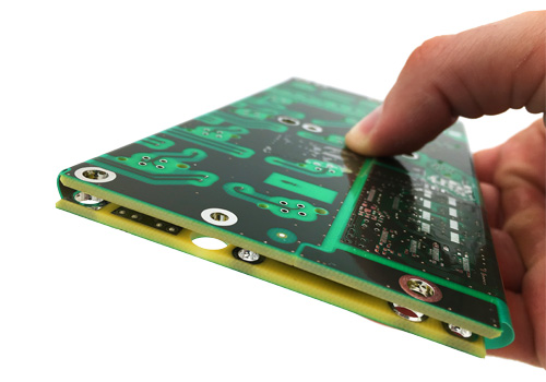
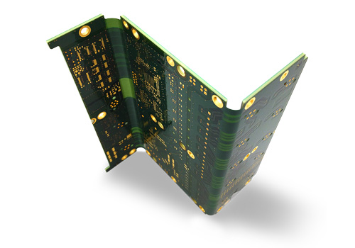
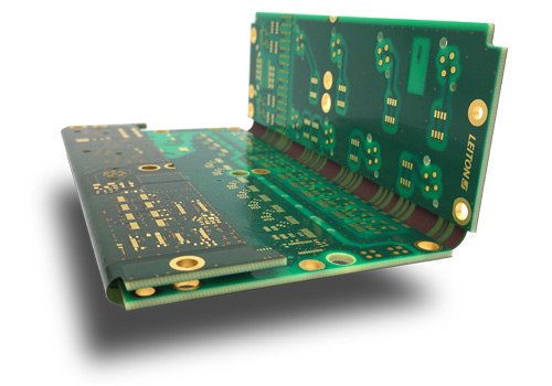
Rigid-flexible printed circuits are PCBs which combine conventional "rigid" circuit boards with flexible parts. A rigid-flexible PCB (RFPCB) can therefore replace several rigid PCBs which otherwise would have to be connected by cables.
This results in the following advantages:
- Often assembly time is reduced significantly
- Many components can be replaced (e.g. connectors, cables, additional PCBs, etc.)
- This allows a higher degree of minituarization
- Reliability increases because especially connectors are possible sources of failures in assembly groups. This is especially valid for products with dynamic movements, during which connectors easily get lose.
On the other side these advantages require a higher price, because production of rigid-flexible PCBs is more complex and moore expensive. However, in many cases the advantages outweigh the higher RFPCB costs when all costs and risks involved are considered.
Which materials are used for rigid-flexible printed circuits (RFPCB) and what does thihs mean for production and assembly?
Rigid-flexible printed circuits consist of a hybrid stack-up. The rigid areas consist of conventional FR4, while the flexible parts are made of polyimide (PI). These tow material types differ not only in bendability but also in a wide range of physical characteristics which have to be considered during manufacturing process. One well-known challenge during production comes with the different heat expansion. The differences have to be anticipated in the layout to assure that after lamination process the layers are aligned perfectly for drilling process. Another challenge lies in the reduced adhesion strength of untreted polyimide compared to FR4. Therefore, polyimide has to be treated with special processes prior to lamination to make its surface more rough.
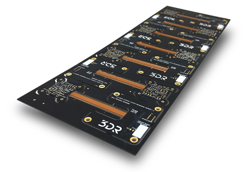
For assembly of rigid-flexible printed circuits one has to take into account that due to the flexible areas assembly of separated units without panel frame will be difficult. In case of automatic (SMT) assembly, it will be even impossible. It is always recommended to design RFPCBs in a panel format, even if it is only one piece. Furthermore, rigid-flexible boards are very hygroscopic - they absorb a lot of humidity. This (very negative) characteristic of polyimide leads to problems during soldering, if the PCBs are not treated properly berfore: trapped humidity causes bubbles, called delamination. For this reason it is extremely important and uninevitable to bake/temper the rigid-flexible boards prior to assembly and soldering. This releases trapped humidity gradually and avoids a temperature shock and bubbles.
Our recommendation based on „ZVEI“ is:
Baking/tempering/drying directly before processing:
- Drying in a convection-, circulating air- or vacuum oven
- Place RFPCBs on grid one by one, do not stack them. You may add high-temeprature paper underneath. IF you use magazines, place them vertically with some distance.
- Drying temperature:130 - 150°C
- Drying time: 120 min
- For thermally sensitive surface finishes (e.g. immersion tin) we recommend a vacuum-drying process because at around 50mbar you may reduce temperature by 20°C and the drying time by 60 minutes.
Direct Processing
- The dried RFPCB must be processed within 8 hours (assembly and soldering).
- Interim storage should be done at 30% (maximum 50%) humidity.
- Always store dry until more soldering steps or repair work is finished.
- If washing processes occurred, follow another drying process according to above parameters.
What bending radius is achievable in the flexible areas?
As a rule of thumb you may apply the following minimum bending radius:
| flex-area | min. bending radius | typical value |
|---|---|---|
| 1-layer outside (O1) | 7 x of flex thickness | 7 x 100µm = 0,7mm |
| 2-layers outside (O2) | 14 x of flex thickness | 14 x 170µm = 2,4mm |
| 1-layer inside (I1) | 7 x of flex thickness | 7 x 140µm = 1,0mm |
| 2-layers inside (I2) | 14 x of flex thickness | 14 x 190µm = 2,7mm |
As rule of thumb keep on mind:
- 1-layer flex >1mm bending radius
- 2-layer flex >3mm bending radius
Apart from above minimum radius please keep on mind that no bending should occur directly at the edge of the rigid part because these edges may act like a tearing-edge and can easily destroy the flexible area.
Please also note that for highly dynamic applications all flexible areas should only consist of rolles-annealed copper. This means that these flexible areas should not receive any plating process and therefore should be inside rather on the outside of the rigid-flexible board. Electrolytic copper deposits are more coarse-grained and therefore break easier than rolled-annealed copper.
Which special technologies are possible for rigid-flexible printed circuit boards?
| special technology | available | comment |
|---|---|---|
| special thickness/stack-up | ||
| express / quick-turn manufacturing | not all types/technologies | |
| up to 12 layers rigid-flexible boards | ||
| special solder mask colours | only in rigid area | |
| 4mil (0,10mm traces) | ||
| 0,10mm drills | only in rigid area | |
| TG170-material | only in rigid area | |
| ENIG/ENEPIG | ||
| connector gold | ||
| peelable mask | ||
| panel production | recommended | |
| press-fit holes | only in rigid area | |
| blind vias | ||
| burried vias | ||
| PTH in flexible areas | not standard, therefore relatively expensive | |
| via-filler | only in rigid area | |
| plated slots | only in rigid area, no plated edge | |
| ALU-IMS-rigid-flex | ||
| Plugging with copper lid (via-in-pad) | for I-stack-ups | |
| copper >35µm | only in rigid area, not in all variations | |
| semi-flex-areas | only in rigid area | |
| impedance control | only in rigid area | |
| HAL-lead free | only I-stack-ups | |
| connectors on inside flexible areas | only I-stack-ups | |
| Rogers-rigid-flex | ||
| UL-logo |
How do rigid-flexible stack-ups generally differ?
In general, there are two main chracteristics of rigid-flexible boards. First, the quantity of flexible layers. Second, the position of the flexible layers. Depending on the supplier there are different nomenclaltures for rigid-flexible boards. One from our perspective useful way of categorizing RFPCBs is to first name the total layer quantity of the rigid part, followed by the position of the flexible layer(s): inner (I) or outer (O). Last, a number specifies how many flexible layers there are.
Some schematic examples will help understanding the nomenclature:
Rigid-flex „4-layer O1“ = 4 layers in total, one flex-layer on the outside (O)

Rigid-flex „4-layers O2“ = 4 layers in total, two flex-layers on the outside (O)

Rigid-flex „4-layer I1“ = 4 layers in total, one flexible layer on the inside (I)

Rigid-flex „4-layer I2“ = 4 layers in total, two flexible layers on the inside (I)

This way of categorizing standard RFPCBs can be extended limitless, e.g. by a „8-layer I4“. It immediately gives a solid idea of complexity and the necessary production steps. In the beginning it is not important whether the flexible layers are layer 2 to layer 5, or centred layer 3 to layer 6. This will be obvious once the layout files are available. It is also not important if some of the rigid layers consist less than the maximum8 layers.
Regarding costs for rigid-flexible printed circuits you can assume that above examples are listed from "less expensive" to "more expensive". Flexible layers on the outside have the advantage during manufacturing that you only need to do the milling process from one side. Single layer flexible circuits have the advantage that you only need to align and cut out coverlay on one side prior to lamination.
What do you have to know when designing rigid-flexible boards?
1 Distance of plated holes (PTH) to flexible areas
Plated drills (PTH) must have a distance of at least 1,0mm from adjecent flexible areas. The reason is that during chemical processing, a lot of fluuids are running through these drills. However, the flexibl area is hollow inside (not laminated). So the only thing keeping chemicals from flowing through the PTH drill and into the hollow part below the flex is this 1,0mm of laminated FR4-PI (in reality due to swelling drills and reducing the prepreg-flow, it is even less than that).
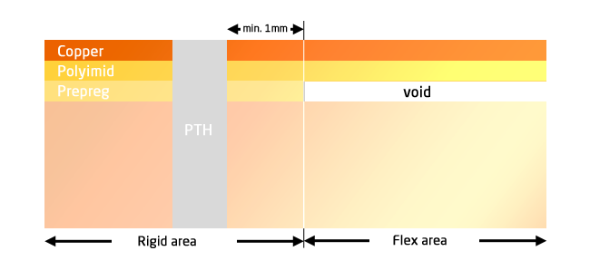
This graphic visualizes the challenge. The FR4 below the FPC will later be milled by z-axis depth milling, so that only the flexible part remains. But if chemicals flew into the hollow part underneath during production, the complete rigid-flexible board is scrap.
2. Traces in the rigid-to-flexible area
All traces coming from the flexible parts should run straight into the rigid area for a length of at least 1,0mm before bending or turning in other directions/angels. This is because in these transition areas the board encounters the highest mechanical strain. Diagonal traces or angels in this transition area create unnecessary sharp angels which tear easily.
3. Traces in flexible areas
In order to maximize bendability of the flexible areas these traces should also run in straight lines. Angels or diagonally running traces may lead to an increased risk of tearing. If there is sufficient space we do recommend additional, thicker traces on to the outside of the flexible areas as a protection against tearing. These trace do not have to have an electrical function but can be inserted as "dummy" traces. However, these traces should also run at least 1,0mm into the rigid area.
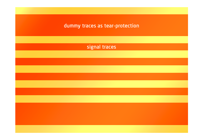
Above graphic shows parallel running traces with thicker dummy traces on the sides. Of course you also decide to put an electrical signal on the outer traces.
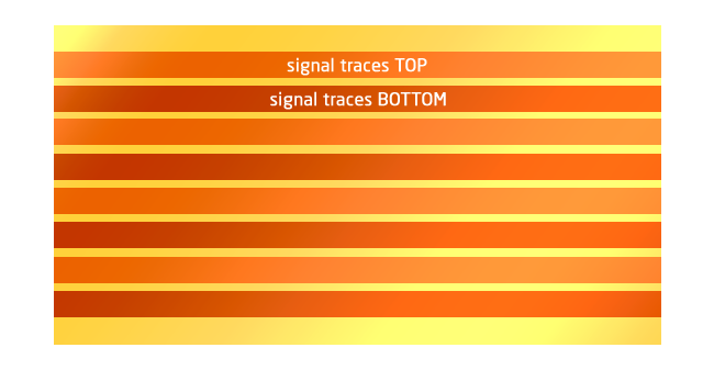
Regardless the stabilizing traces on the sides, for double-sided FPCs all traces should be aligned in a shifted manner so that they do not overlap. This reduces total flexible layer thickness and allows better bending performance.
4. Assembly area
In general, only rigid areas should contain any assembled components because solder-spots easily break in flexible areas when under the slighest strain occurs. To be safe, the distance of any component on the rigid area should at least be 1,0mm away from the flexible area.
5. Panel production
Rigid-flexible boards should always be produced in a panel format. This protects the board during packing and shipment and allows a significantly easier assembly process. If the board is rather big, then it should still be placed in a 1-up panel with additional frames surrounding it. When designing the rigid-flexible board layout you should therefore already include dedicated areas for web-connections which hold the single board inside the panel. These areas cannot be in any flexible area. If you are unusre about the placement of such web-connections please approach us early on and we can help you.
6. Flex-layers in the rigid area
The areas of all flexible layers which will later be inside the rigid stack-up should not contain any large copper areas. Traces or hatched GNB areas are preferrable. The reason is the hygroscopic characteristic of polyimide - it absorbs a lot of humidity during production. This humidity must be removed prior to soldering to avoid delamination. large copper areas in these sections "trap" humidity inside the stack-up and increase the risk of delamination. Furthermore, "ring"-like copper-borders in inner layers should be avoided because they hinder the air from flowing out during lamination.
7. Routing and outline shapes
Always keep on mind that the outline is cut with milling tools. This means that inner corners always consist the routing tool-diameter and cannot be right-angeled. However, in the rigid-flex transition area this is beneficial to stability because a small radius does not tear as easily as a sharp corner. Standard routing tools are either 2,0mm or 1,0mm which results in a radius of 1,0 or 0,5mm respectively.
8. General advice for rigid-flex layouts
As always, try to keep the layout as simple as possible in terms of trace-width and drill-diameters. Wider structures and bigger plated holes may increase durability and reduce production costs at the same time. Keep in mind that while standard rigid PCBs are a "solid and fixed system" after bringing them into service, a rigid-flexible board is often exposed to continuous mechanical stress So it may be wise to include some safety into the layout in terms of robustness, by keeping structures and features as big as possible.

