

up to 8 mm
Thick PCBs | Special Thickness | Super-Thick Boards | up to 8 mm | Thick PCB
Super-thick PCBs in special thicknesses up to 8 mm, multi-press multilayers for test technology, press-fit technology, and mechanical applications
Super-Thick PCBs: Special Thickness up to 8 mm
Leiton manufactures rigid PCBs across a nearly seamless range up to 8.0 mm thickness. These special thicknesses are achieved through multiple pressing cycles. The layer stack-up is individually laminated to the target thickness across several press cycles. A permanently available stock of hundreds of material types supports this, combining various copper thicknesses with properties such as high glass transition temperature (high-Tg) and high tracking resistance (CTI, Comparative Tracking Index).
The bottleneck isn't the material — it's the equipment. Plating lines, drilling machines, and transport systems on standard production lines are typically designed for a maximum board thickness of 4 mm, rarely 6 mm. As a result, most manufacturers simply can't produce PCBs over 4 mm thick, and at 8 mm, nearly all of them drop out. Leiton produces these thicknesses using special equipment.
An honest word of caution: special thickness costs time and money. Multiple pressing cycles and deep-hole drilling extend production time. The aspect ratio limits the smallest possible plated through-hole. If you don't actually need the thickness — mechanically or electrically — standard thicknesses will be more cost-effective.
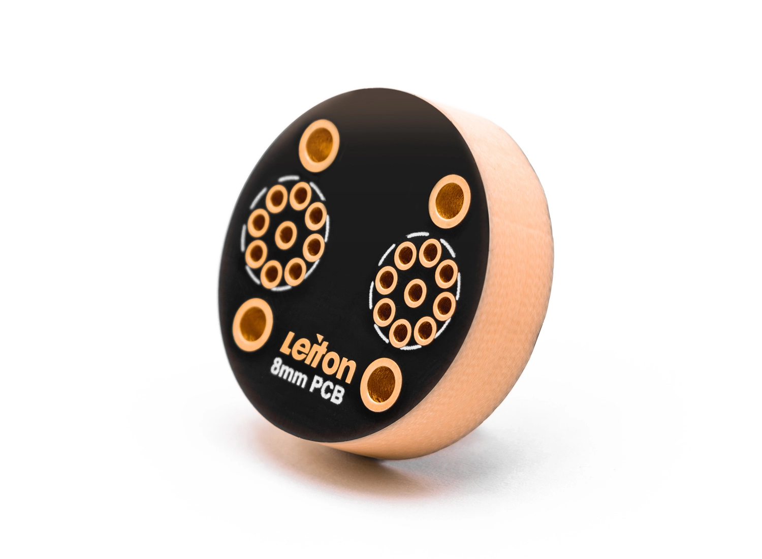
When Should You Use PCBs in Special Thickness?
Special thickness is the right choice when the PCB takes on a mechanical function. If the board carries heavy components, or if it replaces a separate carrier plate as a structural element, special thickness is the appropriate solution. If through-hole technology (THT) requires solid solder joints, long plated-through barrels produce large-area, mechanically robust solder connections.
The reverse also applies: if it's just about rigidity in small form factors, standard thicknesses of 2.4 or 3.2 mm are often sufficient. Special thickness is not a high-current solution. Current-carrying capacity is determined by copper cross-section, not board thickness. An 8 mm thick board with 35 µm outer-layer copper doesn't carry any more current than a standard board. For purely current-related requirements, heavy copper on standard thickness or a busbar are the better-suited solutions.
Applications
Distinguishing Special Thickness from Alternatives
Very thick PCBs compete with solutions that separate mechanical and electrical functions. The table below shows how they compare.
| Solution | Typical Use | When It's the Right Choice |
|---|---|---|
| PCB in special thickness (Leiton, up to 8 mm) | Electrical and mechanical function combined in one component: load-bearing assemblies, press-fit technology, test adapters, heavy-duty THT solder joints. | When the PCB itself takes on a structural/carrier role, when press-fit zones need mechanical support, or when long drilled barrels need to provide mechanically robust solder joints. |
| Standard thickness on carrier plate (aluminum, steel) | Electronics stay standard, mechanical function is solved separately. | When an additional assembly step is acceptable and the PCB itself can remain electrically standard. |
| Heavy copper on standard thickness | High currents without mechanical requirements. | When it's purely about current-carrying capacity, not rigidity or board thickness. |
Advantages
Important Notes:
For plated-through holes, an aspect ratio of 1:8 applies. The minimum plated-through hole diameter is calculated as board thickness divided by 8. At 8 mm thickness, this comes to a minimum of 1.0 mm; at 4 mm, correspondingly 0.5 mm. Multiple pressing cycles and deep-hole drilling noticeably extend lead time compared to standard thicknesses. Costs are above standard as well. V-scoring is not possible on boards over 3 mm, as the scoring process doesn't reach that deep — the contour is routed instead.
During assembly, the high thermal mass must be taken into account; soldering processes and preheating need to be adjusted accordingly. Compliance certificates such as RoHS and REACH are available on request.
Requesting and Calculating Special Thickness
What we need for a solid quote request: target thickness with tolerance, number of layers and copper build-up, smallest plated-through hole, dimensions, material requirements (Tg, CTI), quantity, and Gerber data or a comparable format (ODB++, KiCad, Eagle, etc.). On request, we'll review the layer stack-up and suggest alternatives if standard thickness or heavy copper would solve the requirement more cost-effectively.
Special thicknesses are manufactured by Leiton in Asia, with quality inspections to German standards. Leiton assigns projects according to price, lead time, and technology, from prototype to series production. Why Leiton: special equipment for board thicknesses up to 8 mm, a permanently available material stock with hundreds of types, technical consultation on layer stack-up, CAM inspection (CAM, Computer Aided Manufacturing — preparation and verification of manufacturing data), and personal accessibility.
The industry standard is 1.6 mm, and typical manufacturing processes cover up to about 3.2 mm. From 4 mm onward, most manufacturers reach the limit of their equipment capability — that's where special thickness begins. Leiton manufactures rigid PCBs up to 8.0 mm.
The limiting factor is the equipment's maximum board thickness: plating lines, drilling machines, and transport systems are typically designed for 4 mm, rarely 6 mm. Thicknesses up to 8 mm require special equipment that only a few manufacturers have. The material itself is not the bottleneck.
For plated-through holes, an aspect ratio of 1:8 applies — meaning the smallest plated-through hole equals board thickness divided by 8. At 8 mm thickness, that's 1.0 mm; at 6 mm, it's 0.75 mm; at 4 mm, it's 0.5 mm. Smaller holes can no longer be reliably plated at these depths.
Special thicknesses over 3.2 mm are created by pressing together multiple standard materials. On top of that, deep-hole drilling requires reduced speeds, and contour routing is slower. Each of these steps adds to the lead time, which is why delivery times are noticeably longer than for standard thicknesses.
Material usage (thickness × area), drilling time and tool wear during deep-hole drilling, as well as layer count, panel size, and quantity. Reliable pricing is based on the actual layer stack-up, not on flat-rate figures.
The high thermal mass. The board draws a lot of heat during soldering, so reflow profiles and preheating need to be adjusted. For THT soldering, selective soldering with adjusted preheating or hand soldering with sufficient power output is common. This is manageable, but needs to be planned into the process.
Special thickness is created by pressing standard base materials together. This means the properties of our stock range can be combined — such as high-Tg, high CTI, and various copper thicknesses. Maximum copper thickness is in the range of 200 µm. Plated-through multilayers are also possible in special thickness.

Elektronik-Design
- Expertise through active exchange
- Expertise through training and further education

- ISO 9001:2015 Quality Management
- ISO 14001:2015 Environmental Management

- UL for rigid FR4 PCBs
- UL for flexible circuit boards
- UL for aluminum IMS boards


