BU | PCB | HDI | Sequential Stack-Up
SBU vs. HDI PCBs
HDI (High-Density Interconnect) PCBs and SBU (Sequential Build-Up) technology are often mentioned in the same breath, as if they were directly linked. However, while SBU refers to a clearly defined manufacturing process, HDI mainly describes the result: a compact, fine, and densely packed printed circuit board.
The technologies are intertwined in practice because highly compact boards often require fine drill holes due to space constraints—holes that cannot be produced using only one conventional plated through-hole (PTH) drilling process.
The challenge lies in the so-called aspect ratio, which must be maintained to ensure reliable plating of holes: when holes are narrow but deep, the plating process reaches its limits, as copper cannot be deposited effectively in such geometries.
The solution? Multiple cycles of drilling, plating, and pressing—i.e., a sequential build-up process, or SBU, as explained further below.
Summary:
HDI = fine structures
SBU = several lamination processes
The threshold at which a PCB is considered “High-Density” is constantly shifting due to technological advancements. Just a few years ago, trace widths/spacings of 100µm and drill diameters of 0.20 mm were considered HDI. Today, the term is used for structures starting at 75 µm with 0.10 mm laser-drilled vias in 0.30 mm pads.
Back to the question: can one exist without the other?
Take, for example, a simple 4-layer multilayer PCB that is designed with extreme compactness and pushes the limits of feasible drill sizes and trace widths. This would certainly qualify as HDI. However, with only one lamination cycle possible, it cannot be manufactured using a sequential build-up process—therefore, not an SBU board.
Likewise, thin 6-layer boards with only blind vias might also be HDI but not require SBU processing. SBU boards are more complex and typically only necessary when conventional through-hole drilling, buried vias, or blind vias must reach deep into the board with limited space available. In theory, you could use a sequential build-up process for designs with wide traces and large holes—but technologically, it's unnecessary and economically inefficient.
Conclusion:
HDI without SBU → Possible and not uncommon
SBU without HDI → Possible, but rather uncommon
In practice, SBU PCBs are typically considered HDI, as they are most often used to realize high-density, space-saving designs.
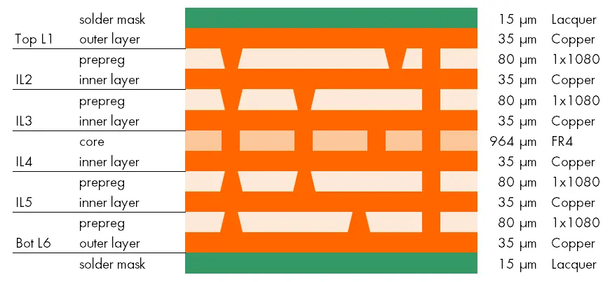
The following explains the process steps of a typical 6-layer SBU multilayer. To illustrate the basic approach, some individual processes are partially combined into a single SBU process step.
The inner layer, which will later be located at the core, is conventionally drilled and plated through.
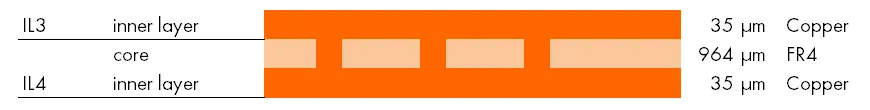
The first lamination is carried out with copper foil on both sides, resulting in a 4-layer multilayer stack.
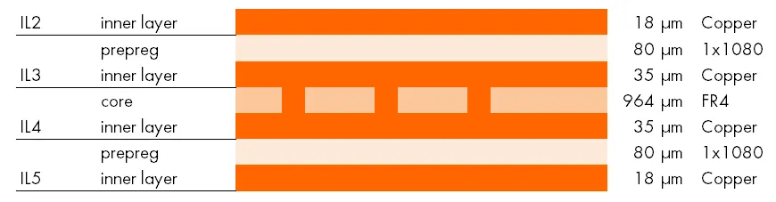
The 4-layer stack is drilled a second and third time, as blind vias must be created from both sides to reach the underlying drill holes—this results in stacked VIAs after the second plating process. The PCB is then patterned (structured) for the second time.
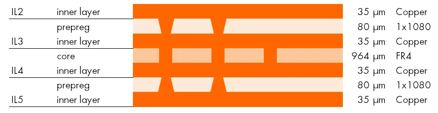
Copper foil is laminated on both sides for the second time to turn the 4-layer multilayer into a 6-layer multilayer stack.
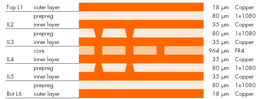
The 6-layer multilayer stack is drilled a fourth and fifth time, as blind vias are once again added from both sides to connect with inner drill holes—this again results in stacked VIAs. Alternatively, standard through-holes can also be drilled through the entire PCB. This is followed by a third plating process and the third patterning (structuring) step.
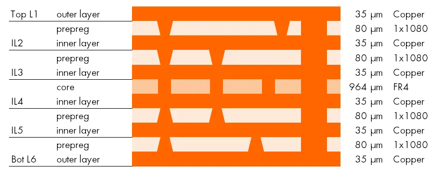
Finally, the completed 6-layer SBU multilayer is surface-finished, coated with solder mask, tested, and routed (milled out).

Elektronik-Design
- Expertise through active exchange
- Expertise through training and further education
- ISO 9001:2015 Quality Management
- ISO 14001:2015 Environmental Management

- UL for rigid FR4 PCBs
- UL for flexible circuit boards
- UL for aluminum IMS boards


