Blind VIA | Buried VIA | PCB | Microvia | Multilayer | Stacked VIA
Blind-, Buried-, Microvia & Stacked & Staggered VIA for PCB
VIAs (Vertical Interconnect Access) enable electrical connections between multiple copper layers of a printed circuit board (PCB). There are different types of VIAs with various advantages and disadvantages, which are selected according to the design requirements.
You can find the corresponding design rules and illustrative diagrams for all VIA types here:
The delivered diameter (i.e., the final diameter) is not the same as the drill diameter. Every PCB manufacturer must enlarge all plated through-holes in the production data to achieve the final delivered diameter.
This is because, during production, a conductive sleeve must be built up inside the plated through-holes to ensure the holes function as electrical connections between the layers.
The aspect ratio describes the relationship between the drill diameter and the drilling depth.
The reason for the aspect ratio requirement lies in the subsequent chemical process steps. If the aspect ratio is too low, air pockets can form in the hole, preventing the plating from being fully built up during the electroplating process. As a result, reliable electrical connectivity through the hole cannot be guaranteed.
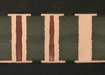
Through-Hole VIAs (PTH) are the fundamental type of vias used in printed circuit boards. In English, they are also referred to as PTH (Plated Through-Holes). Whenever the term "VIA" is used on its own, it typically refers to standard Through-Hole VIAs running from top to bottom. Other types of VIAs are specifically named.
Through-Hole VIAs establish an electrical connection between all copper layers of a printed circuit board, as they penetrate the entire board from top to bottom. They are simpler and more cost-effective to produce than other types of VIAs, as they do not require complex drilling or additional manufacturing steps. However, they occupy more space in the layout, since areas containing VIAs must be kept clear of traces and components on all other copper layers. This limits design flexibility.
For Through-Hole VIAs, an aspect ratio of 1:8 applies. For a standard PCB thickness of 1.55mm to 1.60mm, VIAs must therefore be drilled with a minimum diameter of 0.20mm. In some factories, LeitOn can increase the aspect ratio to 1:10 or more by using specialized machines.
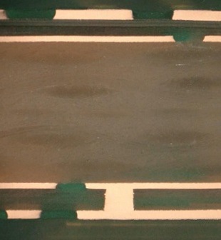
Blind VIAs (blind holes) are VIAs that connect an outer layer with one or more inner layers. They are especially useful in multilayer PCBs where space savings and the minimization of signal interference are important. Since the hole does not go through the entire board, additional traces or components can be placed on layers not reached by the Blind VIA—something not possible with standard Through-Hole VIAs. However, the use of Blind VIAs is subject to type-dependent manufacturing limitations.
Blind VIAs are generally divided into two types:
- Mechanically drilled Blind VIAs
- Laser-drilled Blind VIAs
Mechanically Drilled Blind VIAs are drilled in the same way as regular Through-Hole VIAs. However, an additional Z-depth value is specified for the drilling, since these VIAs should not penetrate the entire PCB. This required Z-depth is determined by the PCB manufacturer.
Mechanically drilled Blind VIAs are less expensive to manufacture than laser-drilled ones, but they require larger drill and pad sizes. Therefore, they are not suitable for PCBs where every tenth of a millimeter counts.
The aspect ratio is the most common limitation when it comes to the feasibility of mechanically drilled Blind VIAs. An aspect ratio of 1:1 is required, meaning the drill diameter must be at least as large as the drilling depth. Especially for Blind VIAs that connect more than one inner layer, the required drill depth makes the VIAs very large, taking up significant space on the PCB.
Another potential issue is the insulation distance behind the target layer of the Blind VIA. To prevent possible voltage breakdown, there must be sufficient insulation between the target layer and the next copper layer. One possible workaround is to remove the copper on the layer immediately behind the target layer in the area of the Blind VIA.
For mechanically drilled Blind VIAs connecting more than one inner layer, not only are larger diameters and pads needed, but also a thicker layer stack. It must also be noted that layer stacks should remain symmetrical to minimize board warping.
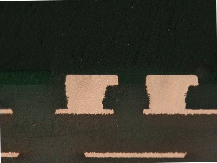
Laser-Drilled Blind VIAs, also called Micro-VIAs or Laser-VIAs, are created by laser drilling rather than mechanical drilling. Since Laser VIAs are typically manufactured with a diameter of 100 µm (0.10 mm), the insulation between the start and target layers must be very thin. A single Prepreg 1080 (65–75 µm) is used for this purpose.
However, because only a thin prepreg is used, it's not possible to realize thicker copper layers (>35 µm) on the inner layers. The thin prepreg would otherwise be insufficient to properly fill the gaps between layers.
Laser Blind VIAs are significantly smaller and therefore require smaller pad sizes, which allows for much tighter layout designs. Typically, Laser VIAs are delivered with a diameter of 0.10 mm in 0.40 mm pads (0.30 mm is also possible). It is often apparent from the layout alone whether Blind VIAs need to be laser-drilled or can be mechanically drilled.
The insulation distance behind the target layer of laser-drilled Blind VIAs is irrelevant, since the laser only minimally hits the copper on the target layer.
Laser VIAs are more expensive than mechanically drilled Blind VIAs.
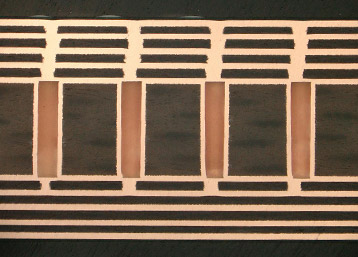
Buried VIAs (buried holes) are VIAs that connect only inner layers and are not visible from the outside. Like Blind VIAs, they are especially useful in multilayer PCBs where space-saving and minimizing signal interference are important. Since they do not pass through the entire board, additional traces or components can be placed on layers not affected by the Buried VIAs—something not possible when using standard Through-Hole VIAs.
Depending on the exact layer stack-up of the PCB and the start and target layers of the Buried VIAs, they are either manufactured like standard Through-Hole VIAs in a 2-layer or multilayer build-up, or like Blind VIAs.
The use of Buried VIAs often requires SBU (Sequential Build-Up) structures. Such stack-ups demand multiple pressing and electroplating processes. Additionally, Buried VIAs often need to be plugged to prevent air pockets during subsequent pressing steps.
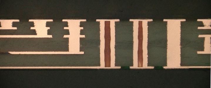
Stacked VIAs (SBU VIAs / Sequential Build-Up VIAs / stacked holes) are a special form of both Blind and Buried VIAs, consisting of multiple VIAs stacked on top of each other. For example, multiple laser-drilled VIAs can be stacked to create Stacked VIAs that could not otherwise be manufactured via conventional drilling or lasering due to aspect ratio constraints.
As with Buried VIAs, Stacked VIAs require multiple pressing and electroplating steps.
One or more layers are pressed onto the existing stack-up layer by layer—always symmetrically on both sides. This process is therefore called SBU, which stands for “Sequential Build-Up”. After each build-up step, the additional drillings (or laser VIAs) are made, plated, and plugged.
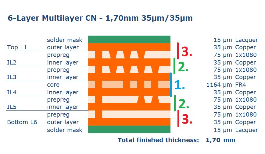
- In the first step, the core VIAs (L3–L4) are drilled, plated, and plugged. These VIAs are manufactured like standard Through-Hole VIAs.
- In the second step, one prepreg and one copper foil are pressed onto both the top and bottom sides. Layers IL2 and IL5 effectively become the new “temporary outer layers” of this SBU stack-up. The Stacked VIAs are then created as if they were laser-drilled Blind VIAs, followed by plating and often plugging.
- Step 2 is then repeated with the same processes. In high-layer-count multilayer PCBs, these steps are repeated accordingly multiple times.
A key advantage of Stacked VIAs is that they ensure reliable electrical connections even with very small VIA sizes, without being limited by the aspect ratio constraints of larger drilled holes. This is especially beneficial compared to mechanically drilled Blind VIAs.
For example, to connect Blind VIAs from Top L1 to IL4 using a mechanical drill, the holes would need to be approximately 1.3 mm in size. Additionally, the layer spacing between IL4 and IL5 would be too small, causing further layout issues. The layer stack would therefore need fundamental changes, and these large Blind VIAs would consume a significant amount of space on the copper layers.
The disadvantage of Stacked VIAs is the significantly higher manufacturing effort due to the many additional process steps, which noticeably increases lead time and cost.
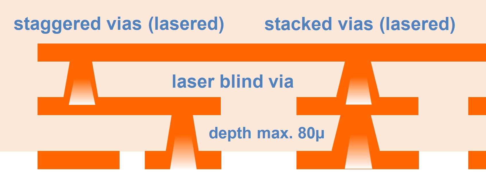
SBU VIAs – “Sequential Build-Up VIAs” (Stacked vs. Staggered VIAs)
Staggered VIAs are a special variant of SBU VIAs. In this case, the VIAs are not stacked directly on top of one another, but each VIA is placed slightly offset, with its own pad next to the VIA below it.
The two methods have different advantages and disadvantages:
| Criterion | Staggered VIAs | Stacked VIAs |
|---|---|---|
| Space Requirement | Higher | Lower |
| Signal Integrity | Good | Potentially better due to more direct signal paths |
| Reliability | Better – less mechanical stress on the VIA wall | Less reliable, especially in high-layer count designs |
| Complexity | Simpler – allows for more relaxed layout tolerances | Requires very precise design, hence more complex |
| Cost | More cost-effective | More expensive |
| Conclusion | A better choice when space is available and ultimate signal integrity is not required | Ideal for limited space or high-performance signal integrity, but costly and less stable if overused |


